








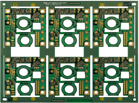
8–32-layer complex bare PCB · typical 5–16 working days Paid 24 / 48-hour expedite · engineering & capacity review required

Complex 8–32-Layer Bare PCB · Prototype & Low Volume

Quick-Turn Complex PCBs—When R&D Cannot Wait.

Urgent projects involving high layer counts, controlled impedance, HDI, high-speed or RF materials, heavy copper or other demanding processes need direct engineering review and tighter schedule control.

MWX PCB focuses on technically demanding 8–32-layer bare PCB prototypes and low-volume builds. Typical production lead times are 5–16 working days, depending on the design, materials, quantity and process requirements.

After 13 years at Q&D Circuits, a publicly listed PCB manufacturer in China, David founded MWX PCB and continues to coordinate engineering, quality and production resources directly for overseas projects.

  • 13 years of factory-side PCB experience
  • Typical 5–16 working-day production
  • Paid 24 / 48-hour expedite by review
MWX / LEAD-TIME REVIEW DESKDAVID REVIEWS DIRECTLY

Fastest feasible schedule

Start with six useful details.

Send your contact details, layer count, quantity, required PCB-ready date and special processes. Gerber or stack-up files are optional for the first contact.

Production time and international transportation are confirmed separately.
ZIP / RAR / 7Z / PDF / XLSX / DOCX / GBR / GER / DRL, maximum 15 MB total

Project notes and uploaded files are treated as confidential from receipt and used only for this inquiry and confirmed project support. Where necessary, disclosure is limited to confirmed engineering or manufacturing resources on a need-to-know basis under confidentiality obligations. Website copies are deleted immediately after the email attempt. See our Privacy Policy. A Mutual NDA is available before file transfer.

David-led project supportOne contact from engineering review through shipment.
Core range8–32-layer complex bare PCB
Typical production5–16 working days
Eligible urgent routePaid 24 / 48-hour expedite

Production schedule reference

Choose the earliest technically credible route.

The normal range and paid expedite options are reviewed separately. A requested date becomes a commitment only after the files, materials, quantity, open EQ items and available capacity are confirmed.

Quick-turn route comparison
RouteBest FitProduction TimeConfirmation
Typical quick-turn8–32-layer complex prototypes and low-volume builds5–16 working daysAfter engineering and material review
Paid 24-hour expediteEligible urgent builds only24 hoursEngineering, capacity, surcharge and PCB-ready date confirmed
Paid 48-hour expediteEligible urgent builds only48 hoursEngineering, capacity, surcharge and PCB-ready date confirmed

Best-fit PCB capabilities

Built for projects a one-click platform cannot simply standardise.

Each design is reviewed as a complete construction: stack-up, materials, via structures, impedance, copper, finish, quantity, inspection scope and the required date.

View capability details
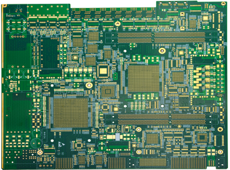
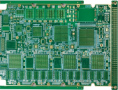
Representative high-multilayer bare PCB 01

High-Multilayer PCB

Best-fit support for technically demanding 8–32-layer prototypes and low-volume builds.

Review focus: Stack-up, materials, copper, controlled impedance and fabrication notes
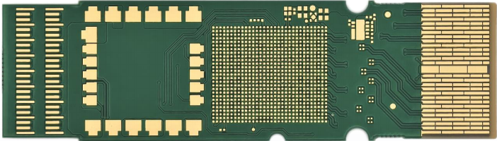
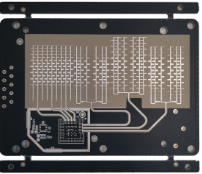
Anonymized 14-layer four-step HDI optical-module manufacturing reference 02

HDI PCB

Blind or buried vias, microvias, via-in-pad, resin plugging and sequential-build structures.

Review focus: Via structure, routing density, plugging, planarisation and stack-up feasibility
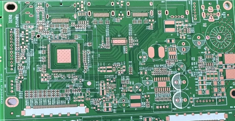
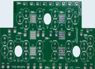
Anonymized 28-layer high-speed PCB manufacturing reference 03

High-Speed & RF PCB

High-speed, RF and microwave projects using controlled stack-ups and selected material systems.

Review focus: Material availability, stack-up, impedance, signal needs and surface finish
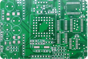
Anonymized eight-layer six-ounce heavy-copper PCB panel 04

Heavy Copper PCB

Power and industrial designs where copper construction, etching and thermal constraints require early review.

Review focus: Copper weight, conductor geometry, resin filling, thickness and inspection needs

Anonymized production references

Real process evidence, with customer identity removed.

These representative manufacturing references come from authorized production-source materials. They show the kinds of technically demanding builds MWX PCB can coordinate; they are not presented as MWX customer claims.

Review all references
Anonymized 14-layer four-step HDI optical-module manufacturing case Open anonymized reference

High-Layer HDI Optical-Module Reference

14 layersIT988GES4 / 4 milImpedance ±5%

Four-step HDI with via-in-pad, resin-plugged vias, controlled-depth drilling and stepped or staggered gold fingers with ENEPIG.

Anonymized 28-layer high-speed PCB manufacturing case using Panasonic M6 Open anonymized reference

28-Layer High-Speed Material Reference

28 layersPanasonic M6High-speed buildMaterial-led review

A representative high-speed board and high-frequency material route showing why stack-up, material availability and process review must be connected to scheduling.

Anonymized eight-layer PCB panel with six-ounce inner and outer copper Open anonymized reference

8-Layer Heavy-Copper Reference

8 layers6 oz inner copper6 oz outer copperBare PCB panel

A representative heavy-copper panel where conductor geometry, etching compensation, finished thickness and inspection scope require project-specific confirmation.

Reference boundary: no customer identity is shown. Final stack-up, materials, tolerance, production time and expedite eligibility are confirmed only after engineering review of the actual project.

01 / Process

A faster path from an urgent requirement to a credible build plan.

One project contact keeps engineering, scheduling, quality and production decisions connected—from first review through shipment follow-up.

STEP 01

Lead-Time Review

Share the layer count, quantity, required PCB-ready date, special processes and any available Gerber or stack-up files. David identifies missing requirements and screens the fastest feasible route.

STEP 02

Engineering & DFM Closure

MWX PCB coordinates the stack-up, material, impedance, process and open EQ review before the production clock or any expedite option is confirmed.

STEP 03

Quick-Turn Bare PCB Build

After technical, commercial and schedule confirmation, MWX PCB coordinates the agreed production route and keeps engineering decisions connected to the build.

STEP 04

Quality & Shipment Follow-Up

David follows the agreed inspection scope, project status, packaging, documentation and international-express handoff through shipment.

Personally managed by David

One accountable contact when engineering time is already tight.

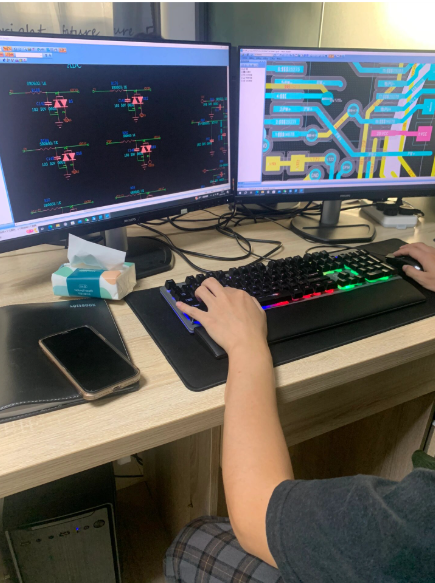
David personally manages Gerber and DFM review, production scheduling, engineering communication, quality-requirement implementation and shipment follow-up.

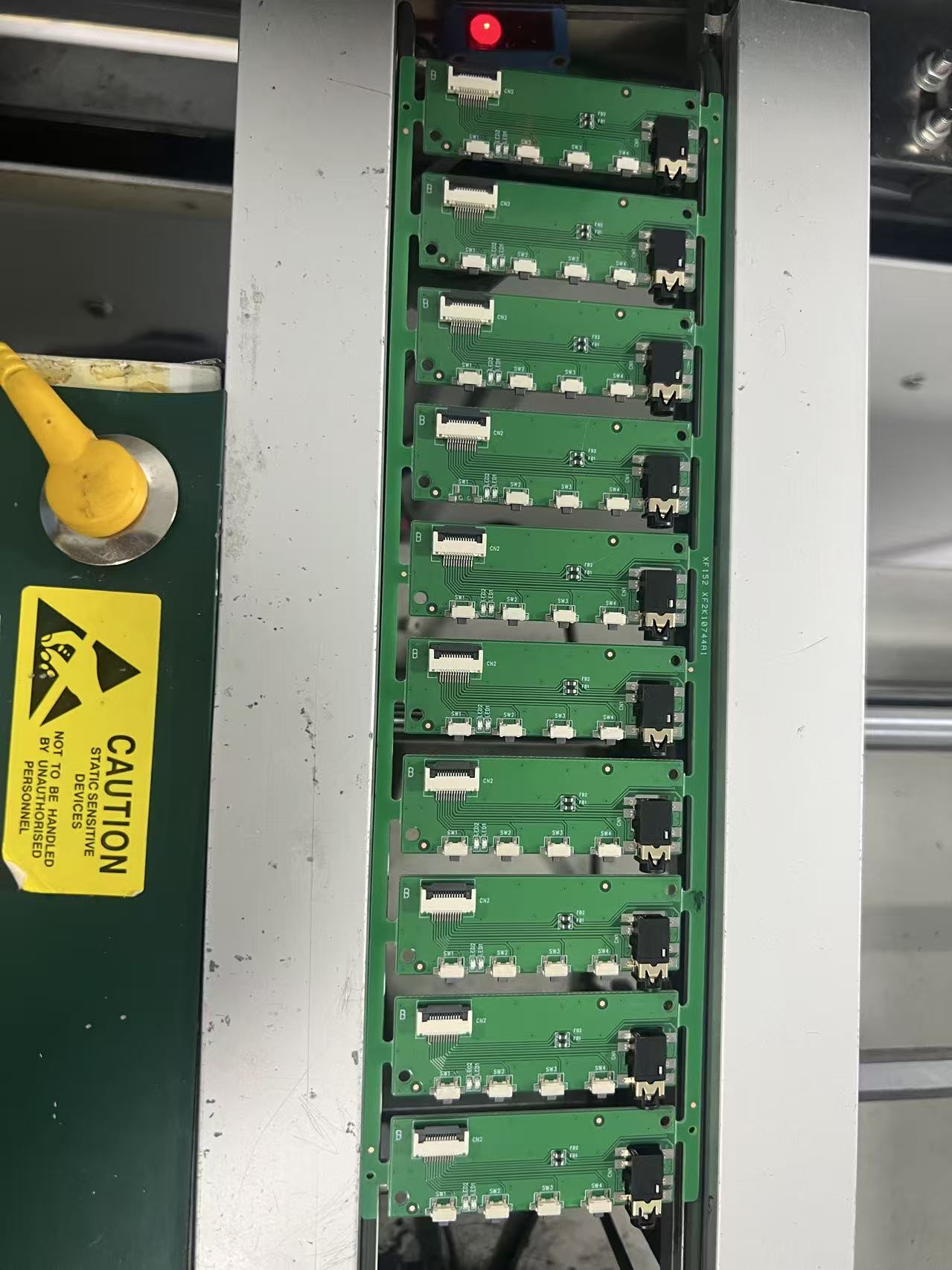
PCB panels being handled on the production floor during manufacturing coordination
Manufacturing coordinationEngineering decisions connected to production action
01 / Customer side

Clear technical and commercial communication

  • Requirements and fabrication-note clarification
  • Quotation, DFM and schedule communication
  • Quality, shipment and issue-resolution follow-up
02 / Production side

Direct engineering and schedule coordination

  • Feasibility, stack-up and process review
  • Capacity and expedited-route assessment
  • Inspection and production-status follow-up

When an engineering, production or quality issue appears, David coordinates the relevant people, decisions and follow-up until the open point is resolved.

See David’s factory-side experience

Quality coordination

Agree what will be checked before the build starts.

Requirements are matched to the design, application risk and production plan. The inspection and documentation scope is confirmed before production release—not added as an assumption afterwards.

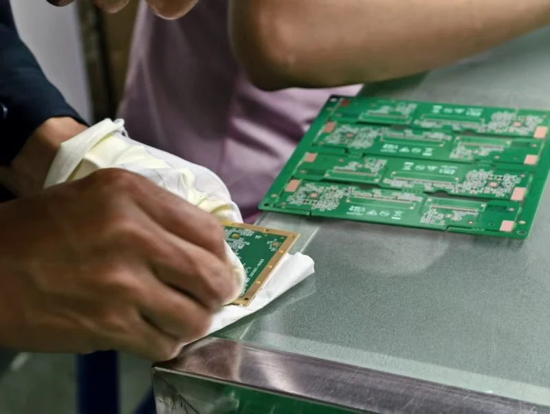
Manual final bare PCB inspection
Representative final bare PCB inspection
01

Requirement & Risk Review

MWX PCB clarifies files, materials, fabrication notes, tolerances, application risk and quality expectations before production.

02

Project-Matched Inspection

Applicable inspection and verification items are coordinated with the responsible quality resources and confirmed for the actual project.

03

Final Shipment Follow-Up

David follows packaging, labelling, shipment details and agreed project records through the final coordination stage.

Review the quality approach

Quick-turn project FAQ

Useful answers before you send an urgent build.

If the files are incomplete, start with the basic project details. The first review identifies the missing items that could block a credible schedule.

Can every 8–32-layer PCB be produced in 24 or 48 hours?

No. The 24-hour and 48-hour routes are separately charged expedite services for eligible projects only. Engineering feasibility, material availability, quantity and current capacity are reviewed before the expedite fee and target PCB-ready date are confirmed.

What does the typical 5–16 working-day range cover?

It is the typical production range for MWX PCB’s core 8–32-layer technically demanding bare PCB prototypes and low-volume builds. The actual schedule depends on the complete design, materials, quantity, process requirements and closure of open engineering questions.

Are rigid-flex and exceptional special-process builds included in that range?

Not as a blanket promise. Rigid-flex, unusual material combinations, extreme copper or build-up requirements and other exceptional constructions are scheduled case by case after engineering review.

Why work with MWX PCB for an urgent R&D build?

David brings 13 years across frontline PCB production, quality, engineering and sales. One accountable contact personally manages the file review, open engineering points, production coordination, quality requirements and shipment follow-up.

What should I send for the first review?

Start with the layer count, quantity, required PCB-ready date and special processes. Gerber files, drill data, fabrication notes and stack-up can be added immediately or after a Mutual NDA is arranged.

Do you provide PCBA or component sourcing?

No. MWX PCB focuses on bare PCB prototypes, NPI and low-volume builds. Assembly, component sourcing and BOM purchasing are outside the service scope.

How are project files protected?

Gerber files and project documents are treated as confidential from receipt and used only for the requested review and project support. Disclosure is limited to confirmed project resources on a need-to-know basis under confidentiality obligations. A Mutual NDA is available before file transfer.

Start with the schedule risk

Send the date your R&D team cannot miss.

Share the layer count, quantity, required PCB-ready date and special processes. Add Gerber and stack-up files now, or arrange a Mutual NDA before file transfer.