HDI PCB manufacturing support
HDI PCB prototypes and low-volume builds with DFM review before production.
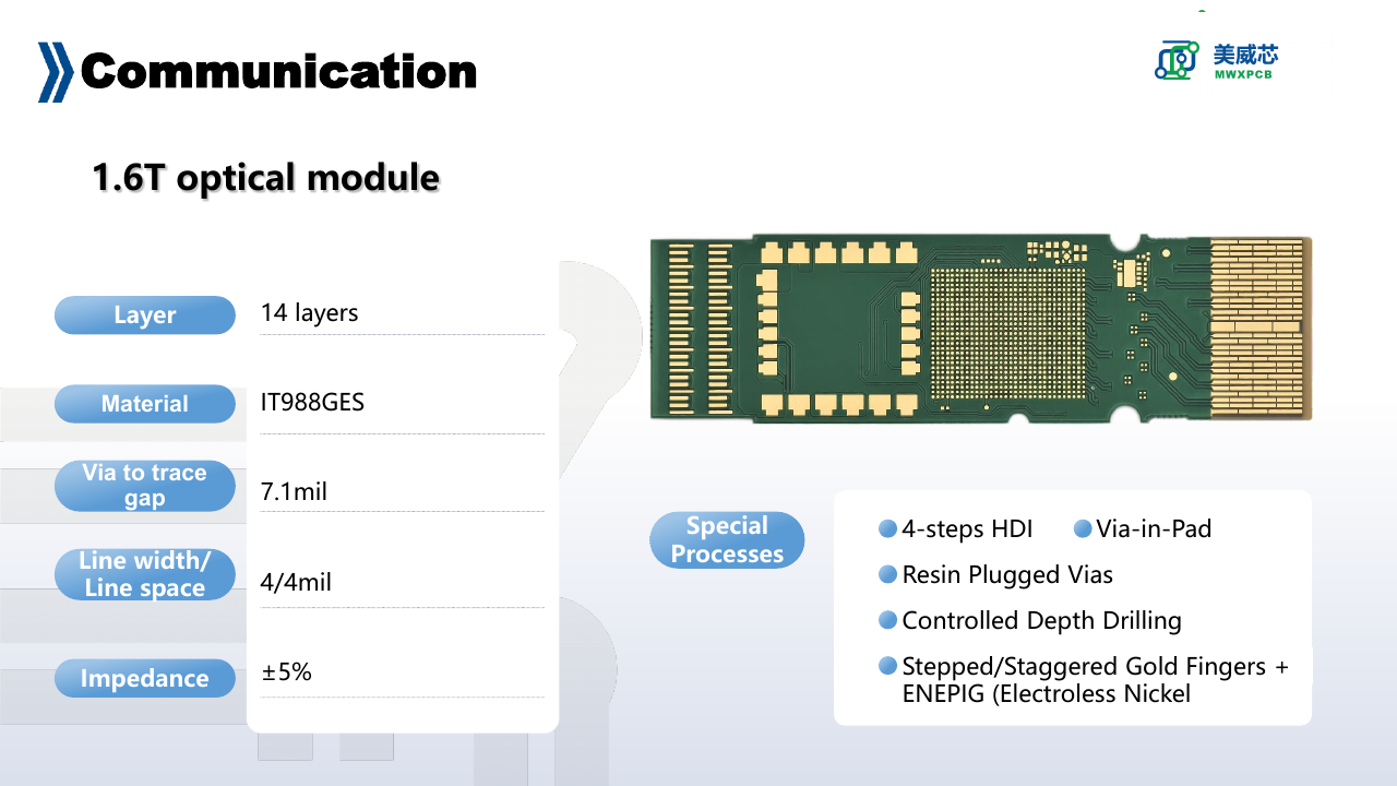
MWX PCB supports overseas engineers with HDI stack-up review, via-in-pad, buried/blind vias, ENEPIG, impedance requirements and practical production follow-up for advanced prototype and low-volume projects.
Best-fit projects
Use this page for advanced HDI work, not commodity PCB orders.
HDI PCB enquiries are valuable when the customer needs real engineering communication: stacked or staggered microvias, via-in-pad, fine-pitch BGA, high-speed routing, thin dielectric control, impedance review or ENEPIG finish.
MWX should position HDI as a DFM-first service. The goal is to confirm stack-up, materials, via structure and process risk before committing lead time or price.
Capability proof
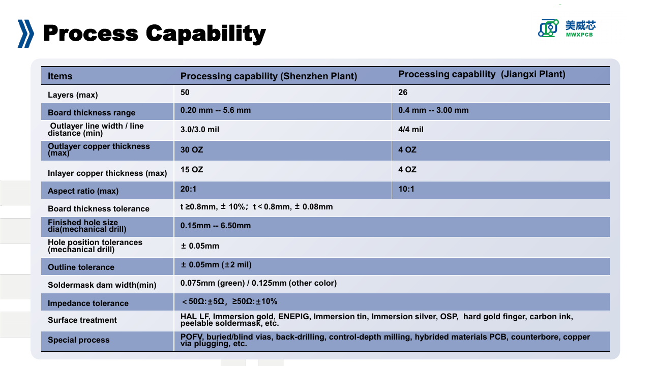
HDI-related process capability used for quotation screening.
| Item | Supported capability |
|---|---|
| Product range | HDI, high multilayer, high-speed and high-frequency PCB support |
| Microvia | 0.075 mm sample laser via; 0.1-0.15 mm production laser via depending on structure |
| HDI structure | Prototype HDI up to 6-step / any-layer review; production route depends on stack-up |
| Special process | Via-in-pad, buried/blind vias, POFV, resin/copper plugging, controlled-depth milling |
| Finish | Immersion gold, ENEPIG, immersion silver, OSP and other finishes after review |
HDI RFQ
Send stack-up, Gerber and via structure for DFM review.
Useful files: Gerber/ODB++, drill files, stack-up, impedance table, BGA pitch, via-in-pad notes, material preference and target lead time.