Complex PCB Manufacturing · PCB Assembly · PCB Layout & DesignShenzhen, China · david.xu@mwxpcb.com

PCB Manufacturing

Need it faster? 24 / 48-hour expedited production is available for qualified PCB projects. Contact us for availability.

Review PCB manufacturing capabilities, lead times, supported materials, process options, and production equipment. PCB assembly and layout design support are also available.

1–50 Layers · HDI · Rigid-Flex · RF / Microwave / Rogers · Heavy Copper · Single- & Double-Sided PCB

Swipe to view all columns

Product ScopeSupported RangeOrder SizeLead-Time Unit
PCB Manufacturing1–50 LayersProject DependentWorking Days

PCB Manufacturing by Product Type

Explore our six PCB product categories. Select a product type to review its manufacturing capabilities, materials, processes and typical lead times.

Manufacturing Capabilities

Process ItemReference Capability
Layers (max)50
Board thickness range0.20–5.60 mm
Outer-layer line width / spacing (min)3.0 / 3.0 mil
Outer-layer copper thickness (max)30 oz
Inner-layer copper thickness (max)15 oz
Aspect ratio (max)20:1
Board thickness tolerancet ≥ 0.8 mm: ±10%; t < 0.8 mm: ±0.08 mm
Finished hole diameter (mechanical drill)0.15–6.50 mm
Hole position tolerance (mechanical drill)±0.05 mm
Outline tolerance±0.05 mm (±2 mil)
Solder mask dam width (min)0.075 mm (green) / 0.125 mm (other colors)
Impedance tolerance<50Ω: ±5Ω; ≥50Ω: ±10%
Surface finishHAL LF, immersion gold, ENEPIG, immersion tin, immersion silver, OSP, hard gold fingers, carbon ink, peelable solder mask, etc.
Special processPOFV, buried / blind vias, back-drilling, controlled-depth milling, hybrid-material PCB, counterbore, copper-via plugging, etc.

Quick-Turn Capability

Reference lead times in working days. Quick-turn orders: ≤1 m². Standard orders: ≤15 m².

8L PCB
Fastest: 3Standard: 7
10L PCB
Fastest: 4Standard: 9

Expedited availability is subject to engineering review and production scheduling.

View Full Lead Times & NotesHide Full Lead Times & Notes

Swipe to view all columns

Product TypeQuick-Turn Production ≤1 m² / OrderStandard Production ≤15 m² / Order
Layer CountFastest Lead TimeStandard Lead Time
2L15
4L25
6L36
8L37
10L49
12L49
14L510
16L511
18L612
20L713
22L814
24L915
26L1016
28L1117
30L1219
32L1321
34L1423
36L1525
38L1627
40L1729
>40LCase by caseCase by case
Volume Production
1–4 Layer Volume ProductionMature Design / Standard ProcessReference Production Lead Time: 12–15 Working Days
Lead-Time Notes
  1. Production lead times are calculated based on a six-working-day week and exclude public holidays.
  2. Lead times do not include time required for customer confirmation of engineering queries or transportation.
  3. The lead times shown are for reference only. Special materials, special processes and complex structures may require additional production time.
  4. For expedited production, engineering conditions and production scheduling must be confirmed in advance.

Materials List

Swipe to view all columns

CategoryModels / Details
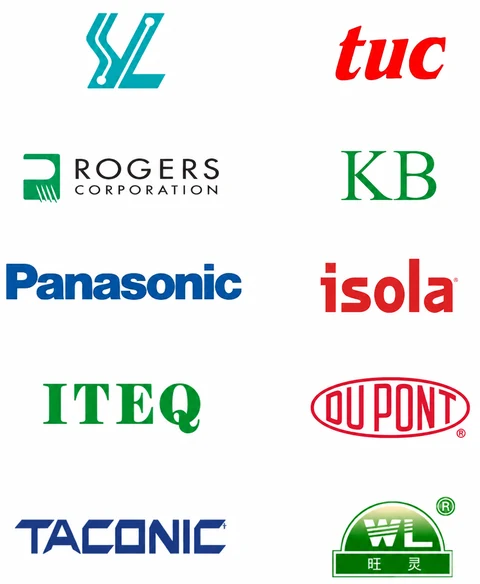
Conventional FR4 SYTECH, TUC, ITEQ, KB S1141/S1000H/S1000-2M; IT-158TC/IT-180ATC; KB-6160/KB-6165G/KB-6167F; TU-768/TU-865; ISOLA 370HR
Halogen free SYTECH, TUC S1150G; TU-747T/TU-865
High frequency SYTECH, TUC, ROGERS, TACONIC, PANASONIC, WANGLING S7135D/S7136; RO3003™/RO4003C™/RO4350B™/RO4730G3/RO5880; AGC TLY-5; ROGERS AD255C™; F4B
High speed SYTECH TU-872 SLK/TU-883/TU-933+; M-4/M-6/M-7; IT-968/IT988G; ISOLA FR408/I-Speed®/Tachyon-100G
High thermal conductivity / High CTI SYTECH, DUPONT ST115G/S1600
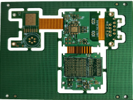
Flexible material PI: SF202/SF305 (Adhesive); AP-85 Series/AP-91 Series; Panasonic R-F775; Coverlay: SF305C

PCB Manufacturing

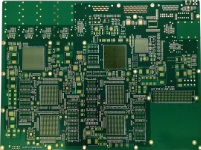
Multilayer & Complex PCB Manufacturing

MWX PCB supports multilayer and high-layer PCB manufacturing for industrial control, communications, computing, power electronics and other demanding applications.

Projects can include controlled impedance, high-speed materials, blind and buried vias, heavy copper and other special process requirements.

HDI PCB Manufacturing

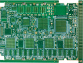
HDI PCB projects can involve microvias, blind and buried vias, via filling and sequential lamination.

Gerber files, stack-up and impedance requirements are reviewed before production to confirm manufacturability and process requirements.

RF & Microwave PCB Manufacturing

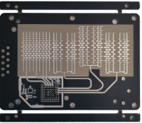
RF and microwave PCB manufacturing requires careful control of laminate selection, dielectric thickness, copper characteristics, impedance and fabrication tolerances.

MWX PCB supports RF PCB projects using specified high-frequency materials such as Rogers and other approved laminates.

PCB Manufacturing Support

Each project can include engineering review, DFM feedback, production follow-up, electrical testing, final inspection, and pre-shipment verification based on project requirements.

We support PCB prototyping, low-volume and volume production, as well as PCB assembly. PCB layout and design support is also available upon request.

Send Us Your PCB Requirements

Upload your Gerber files or share your specifications for engineering review and quotation.

Email us WhatsApp Get a Quote