
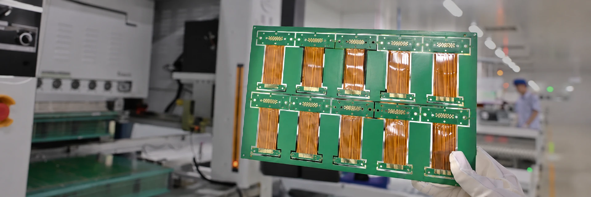
Intended Flexing
A flex-to-install section is formed during assembly and normally remains stationary in service. A dynamically flexing section moves repeatedly, so its construction and mechanical requirements need review against the actual motion.
RIGID-FLEX PCB
We review rigid-flex stack-up, flex materials, bend areas, coverlay and stiffener requirements before quotation.
Please provide fabrication files, the stack-up and flex-zone drawing, bend, stiffener and coverlay notes, assembly outline and component restrictions, and target quantity. We will review manufacturability before quotation.
Rigid and flex sections · transition areas
Bend area · coverlay · stiffeners
Fabrication data · flex-zone drawing · assembly constraints
RIGID-FLEX PROJECT REVIEW
Typical Applications: Industrial control, medical electronics, automotive electronics, robotics, aerospace, and compact electronic systems.
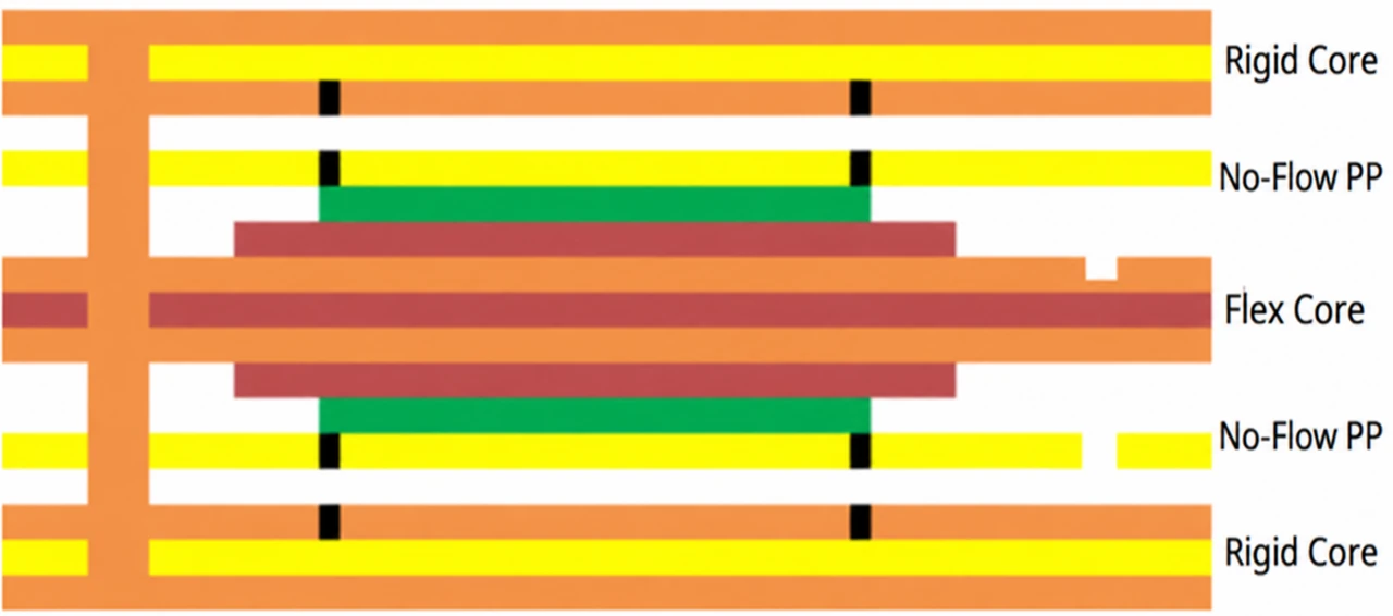
MANUFACTURING DETAILS
A flex-to-install section is formed during assembly and normally remains stationary in service. A dynamically flexing section moves repeatedly, so its construction and mechanical requirements need review against the actual motion.
The rigid-to-flex transition, coverlay openings, and conductor routing are reviewed with the planned bend area. Vias, component pads, and abrupt stiffness changes are generally kept outside the active flex region.
Flex thickness includes polyimide, copper, adhesive, and coverlay layers, each affecting bend behavior. No-flow bonding materials and local stiffeners are selected around the required rigid-flex construction and assembly support needs.
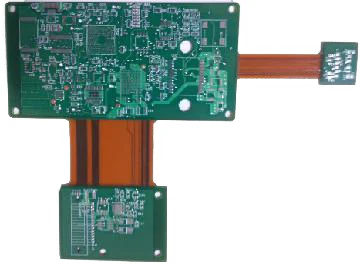
MANUFACTURING EXAMPLE
Flexible tails link separate rigid circuit areas within one board. The transitions, coverlay openings and intended bends are checked with the final mechanical drawing before the construction is released.
| Process Item | Reference Capability |
|---|---|
| Layers | 4–50 layers |
| Coverlay Opening-to-Opening Spacing (min) | 0.2 mm |
| Coverlay-to-Pad Spacing (min) | 0.15 mm |
| Bonding Adhesives | Acrylic / modified acrylic, modified epoxy, and polyimide adhesive |
| FR-4 Application in Multilayer Flex Circuits | Flexible circuits laminated into a rigid-flex board, typically with vias. |
| Solder Mask | Coverlay, LPI |
| Finished Hole Diameter (max) | 6.30 mm |
| Hole-to-Hole Spacing (min) | 0.15 mm |
| Tooling Tolerances | Soft tooling: ±0.25 mm Hard tooling: ±0.05 mm CNC drilling / milling: ±0.10 mm |
| Copper Plating Thickness (PTH Only) | 8–15 μm; 20–30 μm; 30–70 μm (special) |
| Line Width / Spacing (min) | 18 μm finished copper: 3.5 / 3.5 mil 35 μm finished copper: 4.0 / 4.0 mil |
| Coverlay Opening-to-Outline Clearance | 0.20 mm (preferred) |
| Polyimide Film | Per customer requirements: 0.5 mil (12.5 μm) 1 mil (25 μm) 2 mil (50 μm) 3 mil (75 μm) 4 mil (100 μm) 5 mil (125 μm) |
| Copper Foil (RA or ED) | 1/4 oz to 3 oz |
| Stiffeners | Polyimide, rigid FR-4, pressure-sensitive adhesive, metal, or as requested by the customer |
| Finished Hole Diameter (min) | 0.20 mm |
| Hole Diameter Tolerance | ±0.05 mm |
| Conductor-to-Outline Edge Clearance (min) | ≥0.10 mm |
| Layer-to-Layer Misregistration (max) | ±0.10 mm |
| PCB Surface Finish | Immersion Gold, HASL, Lead-Free HASL, Hard Gold, OSP |
Swipe to view all columns
| PCB Specification | Order Area | Standard Lead Time | Fastest Lead Time |
|---|---|---|---|
| 4–40 Layers | ≤15 m² | 5–29 days | 2–17 days |
| 4–40 Layers | >15 m² | Contact us | Contact us |
| Above 40 Layers | Any | Project-specific | Project-specific |
Lead times are based on a six-day working week and exclude public holidays.
Special processes, such as heavy copper foil, peelable solder mask, and blind/buried vias, may require additional production time.
PCB lead time starts from the final confirmation of EQ.
We support 24-hour and 48-hour expedited production.
Please contact us to confirm feasibility and lead time.
Swipe to view all columns
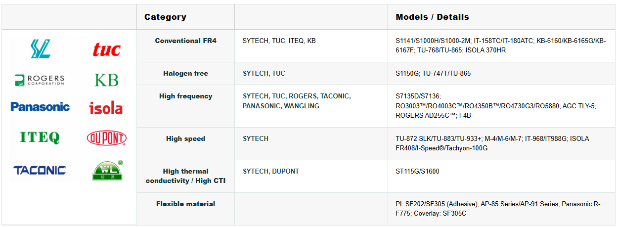
| Category | Manufacturers | Models / Details |
|---|---|---|
| Conventional FR4 | SYTECH, TUC, ITEQ, KB | S1141/S1000H/S1000-2M; IT-158TC/IT-180ATC; KB-6160/KB-6165G/KB-6167F; TU-768/TU-865; ISOLA 370HR |
| Halogen free | SYTECH, TUC | S1150G; TU-747T/TU-865 |
| High frequency | SYTECH, TUC, ROGERS, TACONIC, PANASONIC, WANGLING | S7135D/S7136; RO3003™/RO4003C™/RO4350B™/RO4730G3/RO5880; AGC TLY-5; ROGERS AD255C™; F4B |
| High speed | SYTECH | TU-872 SLK/TU-883/TU-933+; M-4/M-6/M-7; IT-968/IT988G; ISOLA FR408I/I-Speed®/Tachyon-100G |
| High thermal conductivity / High CTI | SYTECH, DUPONT | ST115G/S1600 |
| Flexible material | PI: SF202/SF305 (Adhesive); AP-85 Series/AP-91 Series; Panasonic R-F775; Coverlay: SF305C |
Upload your Gerber files or share your specifications for engineering review and quotation.
You can start with a simple message. No Gerber files are required.
Your message is handled according to our Privacy Policy.
If your email app did not open, copy the address below.
david.xu@mwxpcb.com