
Stack-Up & Materials
Stack-up review covers layer arrangement, board thickness and laminate selection in relation to signal requirements. RF and hybrid constructions also involve the specified material grades and dielectric thicknesses.
Communications PCB projects can combine high-speed interconnects, RF signal paths and dense component layouts. Material selection, stack-up construction, controlled impedance and via structures should be reviewed together before production. MWX PCB supports multilayer and high-layer, HDI, and RF / microwave PCB manufacturing for these applications.

Stack-up review covers layer arrangement, board thickness and laminate selection in relation to signal requirements. RF and hybrid constructions also involve the specified material grades and dielectric thicknesses.
Impedance targets, tolerances and reference layers are assessed alongside the stack-up. The proposed construction and trace geometry are checked against the stated impedance requirements before production.
Via structures and specified back-drilling requirements are reviewed for high-speed interconnects. Fabrication files are checked for clear definitions of features affecting signal paths.
Microvias, blind and buried vias, and via-in-pad are evaluated alongside drilling, filling and lamination requirements. The review covers via types, filling requirements and sequential lamination within the proposed HDI construction.
Copper distribution, finished copper thickness and surface finish are reviewed alongside line, spacing and hole requirements. Specified copper surface characteristics are also considered for RF designs.
Engineering review considers Gerber files, the stack-up, quantities and fabrication notes. DFM feedback helps resolve fabrication questions, while electrical testing and inspection requirements are defined before production.
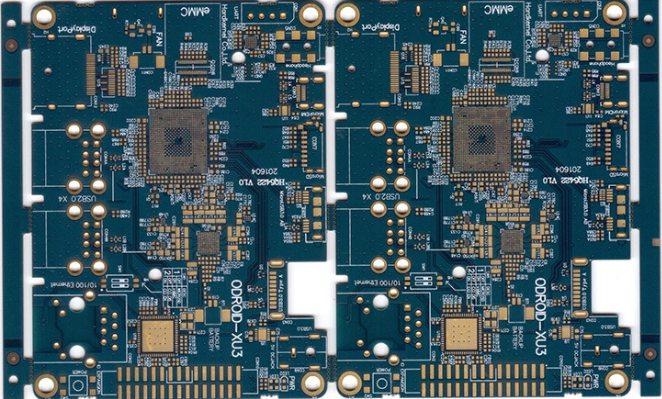
For network switches, routers and other communications boards with complex interconnections. The layer stack-up, copper distribution, impedance requirements and drilling feasibility are reviewed together before production.
Learn More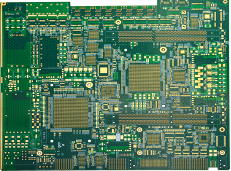
For dense interconnects in compact communication modules. Microvias, via-in-pad and sequential lamination options are reviewed against the proposed stack-up and component layout.
Learn More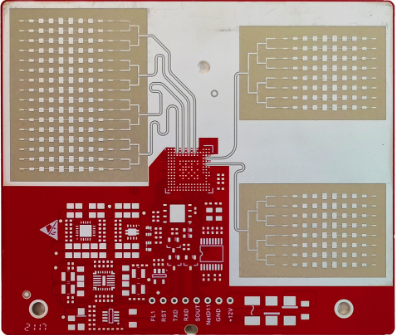
For RF modules, antennas and high-frequency signal paths. Laminate selection, hybrid stack-ups, dielectric thickness and fabrication tolerances need to match the specified RF requirements.
Learn MoreUpload your Gerber files or share your specifications for engineering review and quotation.
You can start with a simple message. No Gerber files are required.
Your message is handled according to our Privacy Policy.
If your email app did not open, copy the address below.
david.xu@mwxpcb.com