
High-Speed Channel Planning
Stack-up details, reference planes, impedance targets and routing constraints are considered for serial links between processors, memory, storage and expansion devices.
Computer and specialized-computing boards combine high-speed interfaces, dense processors, memory and concentrated power demand. Stack-up, return paths, via transitions, copper distribution and thermal paths are considered as one system. MWX PCB supports multilayer and high-layer, HDI, and heavy-copper PCB manufacturing for these boards.

Stack-up details, reference planes, impedance targets and routing constraints are considered for serial links between processors, memory, storage and expansion devices.
Copper weight, plane allocation, via arrays and local power regions are considered together for processor and accelerator networks with concentrated current.
Pad geometry, annular-ring requirements, via types and clearances are considered for fine-pitch processor, memory and controller packages with dense escape routing.
Drill structures, back-drilling notes, stub limitations and via placement are considered where multilayer signal paths cross layers and connector regions.
Finished copper, via filling and heat-spreading features are considered for copper regions, thermal vias and interface areas around heat-producing computing devices.
Layer tables, impedance information, drill data, controlled-depth features and test requirements are coordinated to identify ambiguities affecting the proposed board construction.
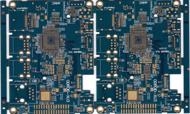
Multilayer and high-layer constructions can suit computer boards that need extensive routing between processors, memory, storage and expansion interfaces. Layer allocation, impedance definitions, power planes and drilling structures are considered against the supplied stack-up and layout.
Learn More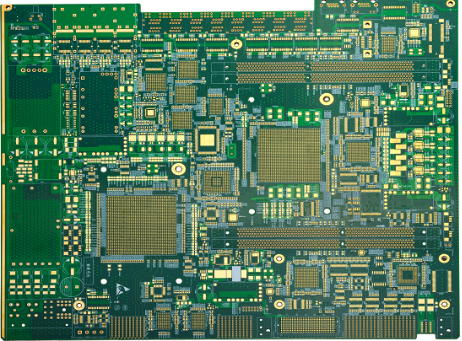
HDI PCB construction can be relevant for compact compute modules and dense BGA escape areas. Microvias, via-in-pad options and sequential build-up requirements are assessed with pad design, routing density and the defined layer transitions.
Learn More
Heavy copper PCB construction can be considered for boards with concentrated power conversion or high-current distribution regions. Copper thickness, plane geometry, plated features and thermal paths are reviewed in relation to the documented electrical and mechanical layout requirements.
Learn MoreUpload your Gerber files or share your specifications for engineering review and quotation.
You can start with a simple message. No Gerber files are required.
Your message is handled according to our Privacy Policy.
If your email app did not open, copy the address below.
david.xu@mwxpcb.com