
Complex PCB Manufacturing · PCB Assembly · PCB Layout & DesignShenzhen, China · david.xu@mwxpcb.com

Multilayer & High-Layer PCB

Multilayer & High-Layer PCB Manufacturing

We review layer count, stack-up, copper distribution, drill and impedance requirements together before quotation.

Multilayer Project Snapshot

Please provide Gerber and NC Drill files, the target stack-up and impedance requirements, and any backdrill notes. We will review manufacturability before quotation.

Layer range

4–50 layers; construction reviewed per project

Engineering checks

Stack-up · impedance · drill and backdrill

File review

Gerber · NC Drill · fabrication notes

MULTILAYER PROJECT REVIEW

Stack-up, Drilling & File Review

  • Stack-up definition: layer order, dielectric construction and copper distribution are reviewed together.
  • Drill and impedance review: hole structure, target impedance and any backdrill stop layers are checked against the design.
  • Gerber review to quotation: submit the fabrication files and requirements for manufacturability review.

Typical Applications: Industrial control, telecommunications, data communication, servers, test equipment, medical electronics, and automotive electronics.

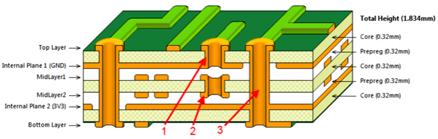
Multilayer PCB stack-up cross-section showing plated through holes, internal planes and layer construction.

MANUFACTURING DETAILS

Multilayer Stack-up and Drilling

Stack-up Definition

A multilayer stack-up defines layer order, dielectric construction, copper distribution, and the intended impedance geometry. Lamination must consolidate the selected cores and prepregs while maintaining registration between the internal circuitry.
Deep-Hole Drill Planning

When a finished hole is deep relative to its diameter, drill selection, chip removal, registration, and hole-wall condition need review together. These factors also affect later cleaning and plated-through-hole preparation.

Backdrill Review

Backdrilling removes an unused plated-through-hole stub after primary drilling and plating, helping reduce discontinuities in selected high-speed signal paths. It is specified separately from the primary drill plan and requires defined stop layers.

MANUFACTURING EXAMPLE

Multilayer PCB Manufacturing Example

28-layer high-speed board

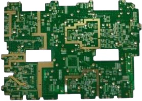
This 28-layer board shows a dense multilayer construction using M6 high-speed material. Layer registration, lamination and plated-hole quality are reviewed as one stack-up rather than as separate process limits.

  • 28 layers
  • M6 material
  • High-speed multilayer construction
Green 28-layer high-speed multilayer PCB with dense component pads and routed features.

Technical Capabilities

Process ItemReference Capability
Layers (max)50
Board thickness range0.20–5.60 mm
Outer-layer line width / spacing (min)3.0 / 3.0 mil
Outer-layer copper thickness (max)30 oz
Inner-layer copper thickness (max)15 oz
Aspect ratio (max)20:1
Board thickness tolerancet ≥ 0.8 mm: ±10%; t < 0.8 mm: ±0.08 mm
Finished hole diameter (mechanical drill)0.15–6.50 mm
Hole position tolerance (mechanical drill)±0.05 mm
Outline tolerance±0.05 mm (±2 mil)
Solder mask dam width (min)0.075 mm (green) / 0.125 mm (other colors)
Impedance tolerance<50Ω: ±5Ω; ≥50Ω: ±10%
Surface finishHAL LF, immersion gold, ENEPIG, immersion tin, immersion silver, OSP, hard gold fingers, carbon ink, peelable solder mask, etc.
Special processPOFV, buried / blind vias, back-drilling, controlled-depth milling, hybrid-material PCB, counterbore, copper-via plugging, etc.
MaterialsHigh-Tg, halogen-free, and Rogers hybrid options

PCB Lead Time

Swipe to view all columns

PCB SpecificationOrder AreaStandard Lead TimeFastest Lead Time
4–40 Layers≤15 m²5–29 days2–17 days
4–40 Layers>15 m²Contact usContact us
Above 40 LayersAnyProject-specificProject-specific

Lead times are based on a six-day working week and exclude public holidays.

Special processes, such as heavy copper foil, peelable solder mask, and blind/buried vias, may require additional production time.

PCB lead time starts from the final confirmation of EQ.

We support 24-hour and 48-hour expedited production.

Please contact us to confirm feasibility and lead time.

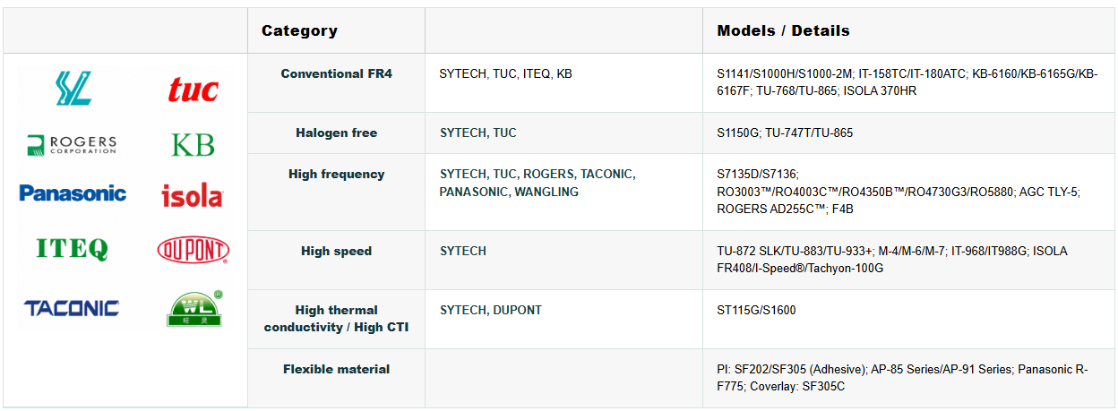
All Supported Materials

Material supplier logos including SYTECH, TUC, Rogers, KB, Panasonic, Isola, ITEQ, DuPont, Taconic and Wangling.

Swipe to view all columns

CategoryManufacturersModels / Details
Conventional FR4SYTECH, TUC, ITEQ, KBS1141/S1000H/S1000-2M; IT-158TC/IT-180ATC; KB-6160/KB-6165G/KB-6167F; TU-768/TU-865; ISOLA 370HR
Halogen freeSYTECH, TUCS1150G; TU-747T/TU-865
High frequencySYTECH, TUC, ROGERS, TACONIC, PANASONIC, WANGLINGS7135D/S7136; RO3003™/RO4003C™/RO4350B™/RO4730G3/RO5880; AGC TLY-5; ROGERS AD255C™; F4B
High speedSYTECHTU-872 SLK/TU-883/TU-933+; M-4/M-6/M-7; IT-968/IT988G; ISOLA FR408I/I-Speed®/Tachyon-100G
High thermal conductivity / High CTISYTECH, DUPONTST115G/S1600
Flexible materialPI: SF202/SF305 (Adhesive); AP-85 Series/AP-91 Series; Panasonic R-F775; Coverlay: SF305C

Send Us Your PCB Requirements

Upload your Gerber files or share your specifications for engineering review and quotation.

Email us WhatsApp Get a Quote