
Current Path Definition
Copper weight, conductor geometry and plated-hole details are considered for current-carrying traces, pours, vias and terminals in power conversion and distribution boards.
Power and energy boards combine high-current paths, switching nodes, control circuits and large connected components. PCB construction considers current paths, insulation-related spacing, thermal interfaces and connector geometry. MWX PCB supports heavy-copper, multilayer and high-layer, and double-sided PCB manufacturing for these applications.

Copper weight, conductor geometry and plated-hole details are considered for current-carrying traces, pours, vias and terminals in power conversion and distribution boards.
Component placement, loop geometry and power-return relationships are considered with copper patterns, layer assignment and drill features for fast switching circuits.
Specified copper areas, thermal vias, internal planes and exposed-pad features are considered for localized heat from power semiconductors, magnetics and current-sense elements.
Defined clearances, slots, cut-outs and copper keep-outs are considered with board outline and layer information for high-potential nodes, isolation boundaries and connectors.
Finished-hole specifications, annular-ring expectations, slots and reinforcement features are considered with board thickness and copper construction for busbars, terminals and large capacitors.
Gerber files, drill data, stack-up notes and assembly-interface drawings are coordinated for board outline, copper features, hole definitions and requested testing.
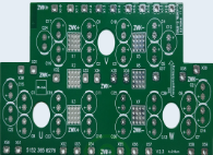
Suitable for power paths that use larger copper areas, robust terminals or concentrated current transitions. Heavy-copper PCB construction can be discussed using the proposed trace geometry, plated holes, layer count, thermal features and associated fabrication notes.
Learn More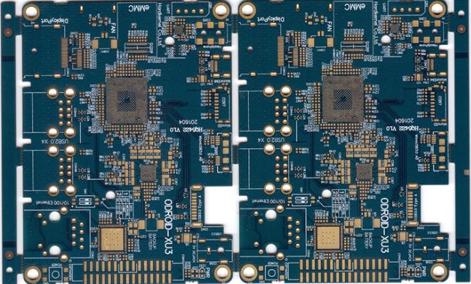
Suitable for power-control assemblies that need separate routing layers for control, sensing, communication and distribution functions. A multilayer stack-up can organize these functions within one board; dielectric choices, copper distribution and isolation features are evaluated from supplied fabrication requirements.
Learn More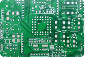
Suitable for simpler power-interface, monitoring or auxiliary-control boards with routing on two copper layers. Double-sided construction can support defined connector, switching and measurement sections where the supplied layout allows sufficient routing, thermal copper and required mechanical features.
Learn MoreUpload your Gerber files or share your specifications for engineering review and quotation.
You can start with a simple message. No Gerber files are required.
Your message is handled according to our Privacy Policy.
If your email app did not open, copy the address below.
david.xu@mwxpcb.com