
Precision Analog Partitioning
Layer arrangement and copper layout are considered for defined analog regions, return paths and keep-outs around references, amplifiers, filters, converters and digital control.
Test and measurement boards combine low-level analog inputs, high-speed conversion, RF paths and dense digital processing. PCB construction considers signal partitions, reference structures, connector geometry and fixture access. MWX PCB supports multilayer and high-layer, RF and microwave, and HDI PCB manufacturing for these applications.
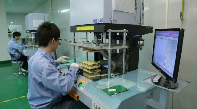
Layer arrangement and copper layout are considered for defined analog regions, return paths and keep-outs around references, amplifiers, filters, converters and digital control.
Stack-up details, trace escape areas, via structures and reference-plane continuity are considered for sensor inputs, multiplexed paths, converter interfaces and timing signals.
Specified impedance targets, layer references, trace definitions and drilling features are considered for fast converter interfaces and processing links.
Material callouts, dielectric dimensions, copper features and connector footprints are considered for controlled RF paths, shielding interfaces and high-frequency connectors.
Board outline, edge plating, holes, test pads, fiducials and local clearances are considered for instrument and fixture connections at edges, headers and probe fields.
Fabrication drawings, stack-up notes, panel restrictions and inspection information are coordinated with Gerber files and drill data for dimensions, special features and test definitions.
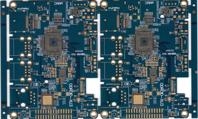
Suitable for acquisition and instrumentation boards that integrate analog front ends, converters, processors, memory and multiple interface sections. Multilayer construction can provide routing space and reference planes; stack-up, impedance features, copper balance and drilling details are evaluated from the submitted fabrication package.
Learn More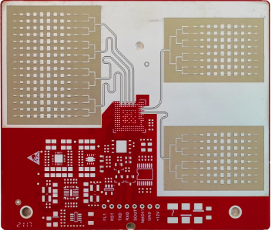
Suitable for test modules with RF signal paths, high-frequency connectors, antennas or shield interfaces. RF and microwave constructions can be considered from the specified laminate, dielectric geometry, copper characteristics, controlled features and connector interface requirements.
Learn More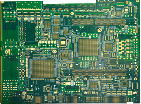
Suitable for compact acquisition modules with fine-pitch converters, dense processor escape routing or closely spaced connectors. HDI options can be reviewed with the proposed pad pattern, microvia structure, build-up sequence and land-pattern requirements documented for the specific board.
Learn MoreUpload your Gerber files or share your specifications for engineering review and quotation.
You can start with a simple message. No Gerber files are required.
Your message is handled according to our Privacy Policy.
If your email app did not open, copy the address below.
david.xu@mwxpcb.com