
Instrument Mixed-Signal Layout
Stack-up, copper partitions, return structures and keep-outs are considered for diagnostic and monitoring instruments combining analog acquisition, digital control, displays and local power.
Medical device electronics combine precision sensing, imaging signal chains, interfaces, wireless functions and power management in compact assemblies. PCB manufacturing considers mixed-signal separation, dense interconnects, thermal paths and flexible sections. MWX PCB supports multilayer and high-layer, HDI, and rigid-flex PCB manufacturing for these board types.

Stack-up, copper partitions, return structures and keep-outs are considered for diagnostic and monitoring instruments combining analog acquisition, digital control, displays and local power.
Layer build-up, escape routing, via structures and reference-plane placement are considered for sensor, analog-front-end, conversion and processing circuits in compact imaging electronics.
Pad geometry, drilling, component-side clearances, board thickness and routing density are considered for portable equipment with fine-pitch components and tightly spaced connectors.
Specified copper regions, thermal vias, internal planes and exposed-pad features are considered for concentrated thermal and current paths around processors, displays and power devices.
Bend areas, coverlay, stiffeners, transition geometry, copper features and connector interfaces are considered for rigid-flex sections across folded or space-limited mechanical zones.
Revision-controlled drawings, material notes, identification requirements and inspection records are coordinated with Gerber files, stack-up, drill data and fabrication notes.
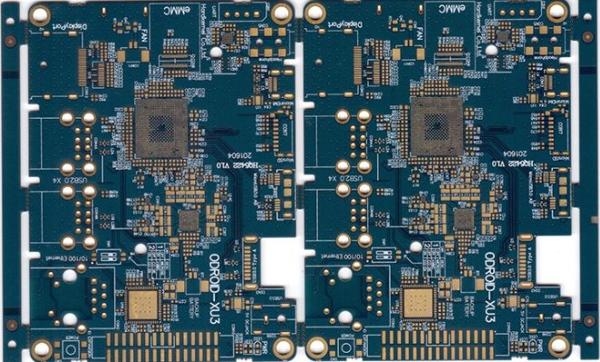
Suitable for complex instrument boards that combine signal acquisition, processing, display or communication functions. A multilayer stack-up can organize dense routing and reference planes; the selected layer arrangement, copper distribution, impedance features and drill details follow the supplied program documentation.
Learn More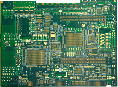
Suitable for compact modules using fine-pitch processors, converters, memory or dense connector interfaces. HDI features can be evaluated from the proposed pad design, microvia structure, layer build-up, assembly land patterns and related drilling details.
Learn More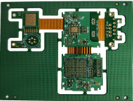
Suitable for assemblies that route between compact mechanical zones or integrate fixed and flexible circuit sections. Rigid-flex construction can be discussed from bend geometry, stiffeners, coverlay, layer transitions and mechanical drawings supplied for the specific device module.
Learn MoreUpload your Gerber files or share your specifications for engineering review and quotation.
You can start with a simple message. No Gerber files are required.
Your message is handled according to our Privacy Policy.
If your email app did not open, copy the address below.
david.xu@mwxpcb.com