
Sensor Signal Paths
Component placement, grounding regions, trace routing and return paths are considered for sensor nodes combining low-level analog inputs, digital processing and power circuitry.
IoT and artificial-intelligence hardware links sensors, wireless interfaces, local processing and power management in compact products. PCB construction considers antenna areas, mixed-signal routing, dense packages, flexible interconnects and mechanical constraints. MWX PCB supports HDI, RF / microwave, and rigid-flex PCB manufacturing for IoT and edge-processing hardware.

Component placement, grounding regions, trace routing and return paths are considered for sensor nodes combining low-level analog inputs, digital processing and power circuitry.
Material selection, copper keep-outs, ground treatment, controlled-impedance traces and interface geometry are considered for antennas, radio modules and RF connectors.
Fine-pitch escape routing, microvia options, pad design and layer transitions are considered for processors, memory, sensors and connectivity devices in compact edge AI products.
Bend regions, stiffeners, connector locations, copper features and rigid-to-flex transitions are considered for wearable, camera and constrained enclosure designs.
Copper regions, via placement, switching-area separation and component clearances are considered for battery-operated or distributed sensor equipment with charging, regulation and radio loads.
Outline geometry, mounting points, connector access, edge clearances and specified coating or handling requirements are considered for restricted enclosures, instruments and field-mounted assemblies.
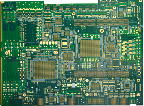
HDI PCB types can suit compact sensor hubs and edge-processing modules with dense packages. Microvias, via-in-pad options and sequential build-up structures are evaluated with component footprints, routing escape requirements and the board interconnection plan.
Learn More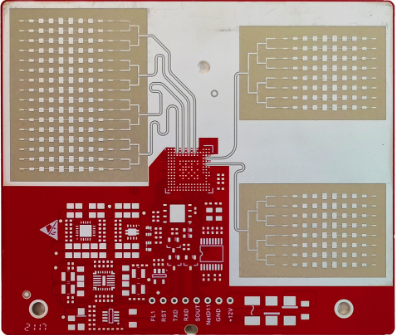
RF and microwave PCB types can be considered for wireless modules, antenna feeds and radio-interface sections. Laminate choice, dielectric construction, controlled impedance and copper geometry are reviewed against the supplied RF layout requirements and system interfaces.
Learn More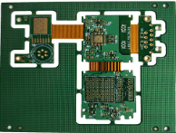
Rigid-flex PCB types can support products that connect sensors, displays or cameras across a constrained enclosure. Rigid and flex layer definitions, bend areas, stiffeners and connector transitions are assessed in relation to the mechanical design package.
Learn MoreUpload your Gerber files or share your specifications for engineering review and quotation.
You can start with a simple message. No Gerber files are required.
Your message is handled according to our Privacy Policy.
If your email app did not open, copy the address below.
david.xu@mwxpcb.com