
Resin-Filled Vias, Solder-Mask-Plugged Vias and Via-in-Pad
Resin filling, solder-mask plugging and via-in-pad describe different requirements. The right construction depends on the via location, assembly and fabrication process.
Resin-filled vias, solder-mask-plugged vias, and via-in-pad are related terms, but they describe different things. Treating them as interchangeable can lead to soldering defects, unclear fabrication data, or an unnecessarily expensive board build.
Resin-Filled Vias
A resin-filled via has its plated hole barrel filled with an epoxy-based material. The fill may be non-conductive or conductive, depending on the required construction and the fabricator’s qualified process. The term “filled” alone does not specify the material, degree of fill, or final surface treatment.
Resin filling can limit the entry of solder or process fluids into a via and support a more planar surface for further processing. When a solderable component pad is formed over the via, a common solution is to fill and planarize the hole, then plate a copper cap over it. The required sequence depends on the via structure and board stackup.
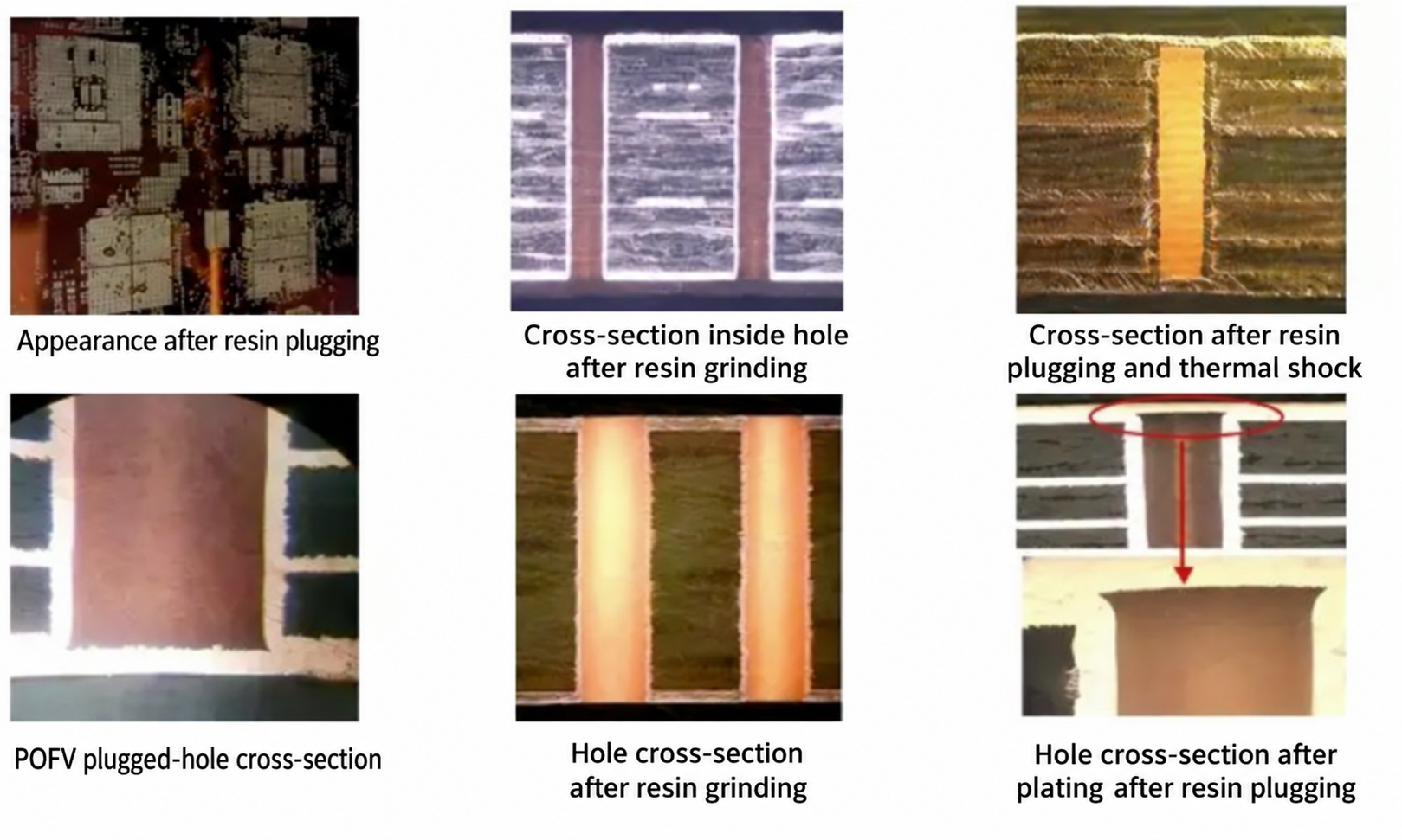
Filling adds manufacturing steps and cost. Feasibility depends on the hole dimensions, aspect ratio, via type, copper structure, materials, and the board shop’s process. The fabrication data needs to identify which vias require filling; a local drill-file naming convention does not define a universal process.
Solder-Mask-Plugged Vias
A solder-mask-plugged via is closed by applying liquid solder mask to the hole. This is a via-protection method with a different construction from a resin-filled and copper-capped via. It can help limit solder wicking or unwanted material entering selected vias, subject to the board design and the fabricator’s process.
Plugging depends on hole geometry, mask material, application and curing. Partial plugs, shrinkage, trapped residues, or mask defects can affect the result. Availability and acceptance criteria also vary by manufacturer and surface finish. A mask plug alone does not provide the flat, exposed copper surface normally required for a solderable component pad.
Via-in-Pad
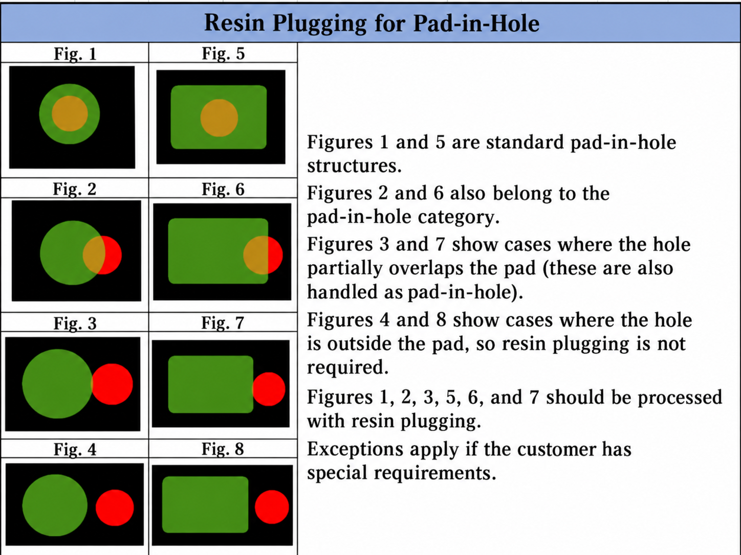
Via-in-pad describes the position of a via within a component pad. It does not, by itself, specify whether that via remains open or receives resin fill, copper fill, a copper cap, or another treatment.
An open via in a pad that will be soldered can draw solder away from the joint and leave an uneven landing surface. A filled, planarized, copper-capped via-in-pad construction is a common way to provide a flat solderable pad. It can be relevant to fine-pitch BGA routing, dense interconnects, or selected thermal-pad designs. The correct treatment follows the pad’s actual assembly and routing requirements, rather than a blanket rule for every BGA.
Manufacturing Review
- Via definition: Which vias are affected, where they terminate, their finished hole sizes and their relationship to component pads.
- Required treatment: Mask plugging, resin filling, conductive fill, copper capping, or a specified combination.
- Finished surface: Whether the location needs a flat, solderable copper pad and which surface finish will be applied.
- Fabrication and assembly: Stackup compatibility, planarity, inspection criteria, solder-wicking risk, and process cost.
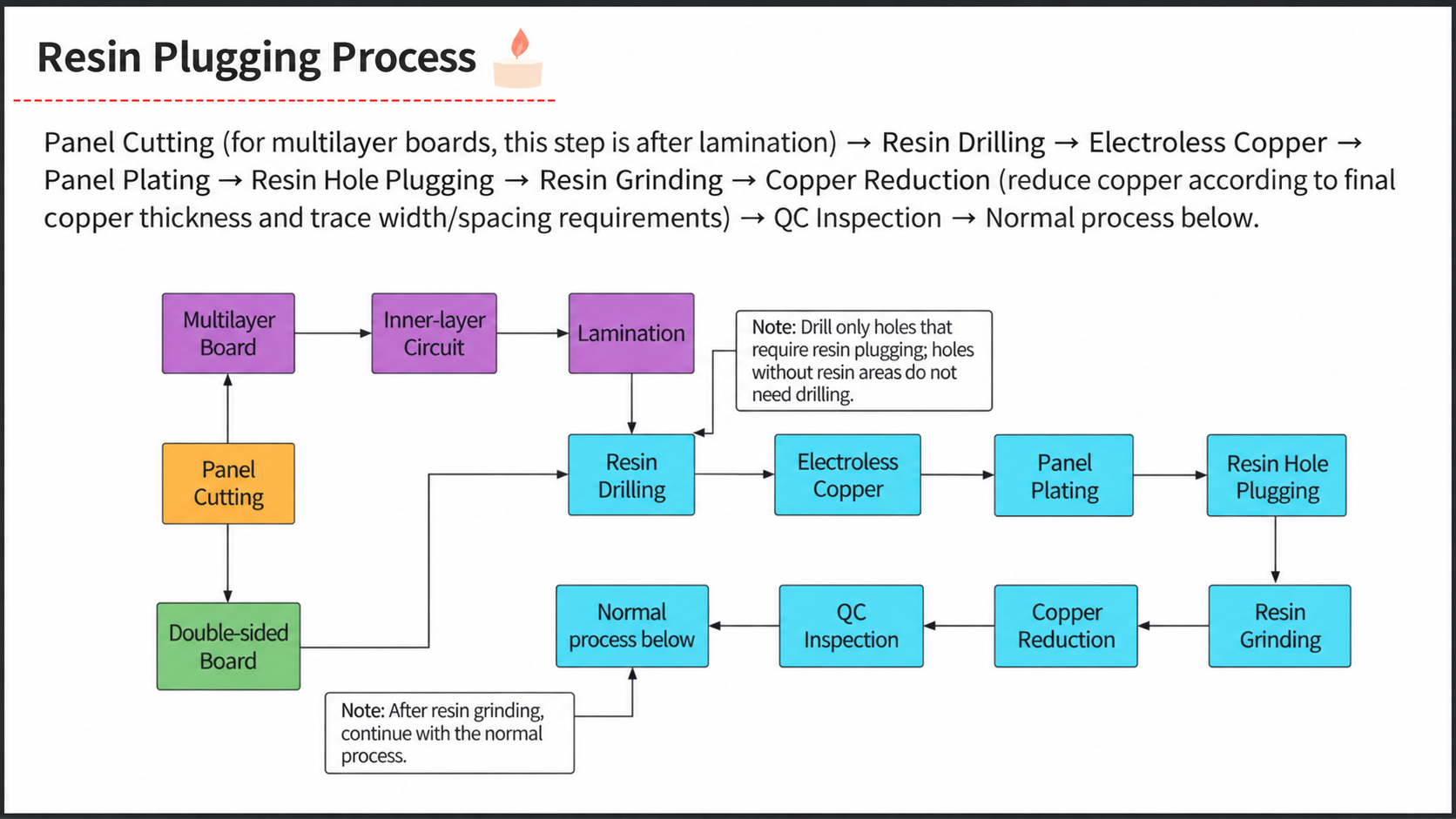
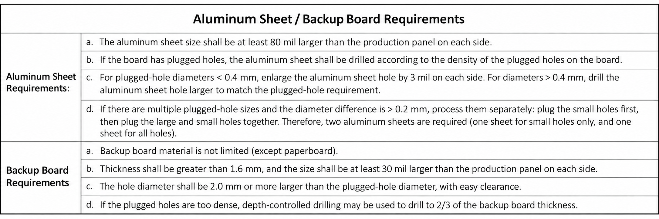
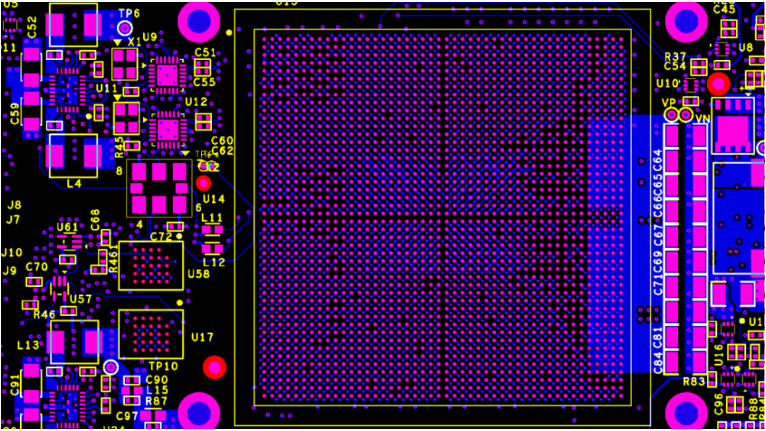
These separate definitions make the fabrication request clearer and allow the via treatment to be checked against the intended assembly and the manufacturer’s actual capability.
BACK TO TECHNICAL ARTICLES