
HDI Stacked vs. Staggered Microvias: What to Confirm Before Choosing a Structure
Compare layer spans, routing space, via filling, sequential build-up and reliability when choosing an HDI stacked or staggered microvia structure.
HDI construction is defined by the interconnections the design needs, not simply by the total number of PCB layers. Plated through-holes, buried vias and laser-formed microvias may appear in the same board. When two adjacent microvia levels are required, their positions determine whether the route is staggered or stacked. That choice affects routing density, build sequence, via treatment and reliability review.
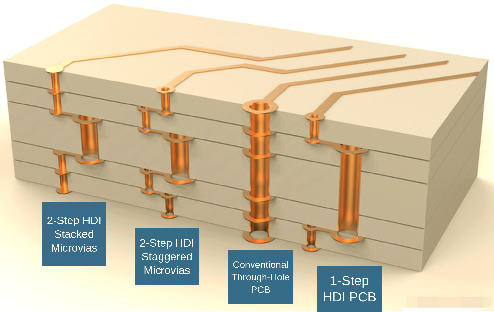
Start with the Required Layer Connections
A plated through-hole connects the outer surfaces and can contact selected internal layers. Its presence does not make the board non-HDI: a design can combine through-holes with one or more microvia build-up stages. The first review identifies each required start and end layer, which nets need fine-pitch escape, and where a conventional drilled hole would consume too much routing space. For a project-specific build-up and file review, see HDI PCB manufacturing.
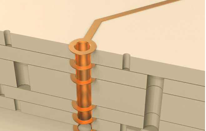
One-Stage HDI and Sequential Build-Up
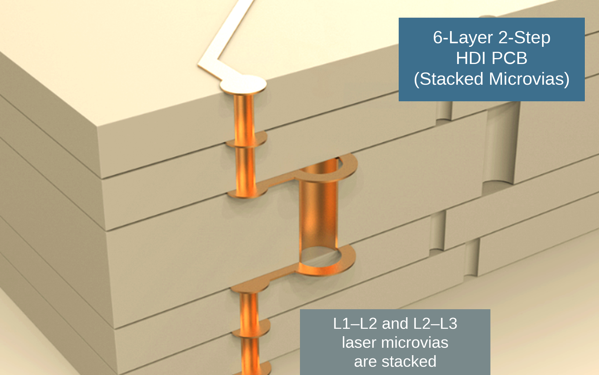
A one-stage HDI construction adds one microvia level on one or both sides of a central structure. In the illustrated six-layer example, outer laser microvias connect L1–L2 and L5–L6, while an internal mechanical via connects layers within the core. The actual drill spans and lamination sequence must be stated in the stackup; a label such as “one-step HDI” alone is not enough manufacturing data.
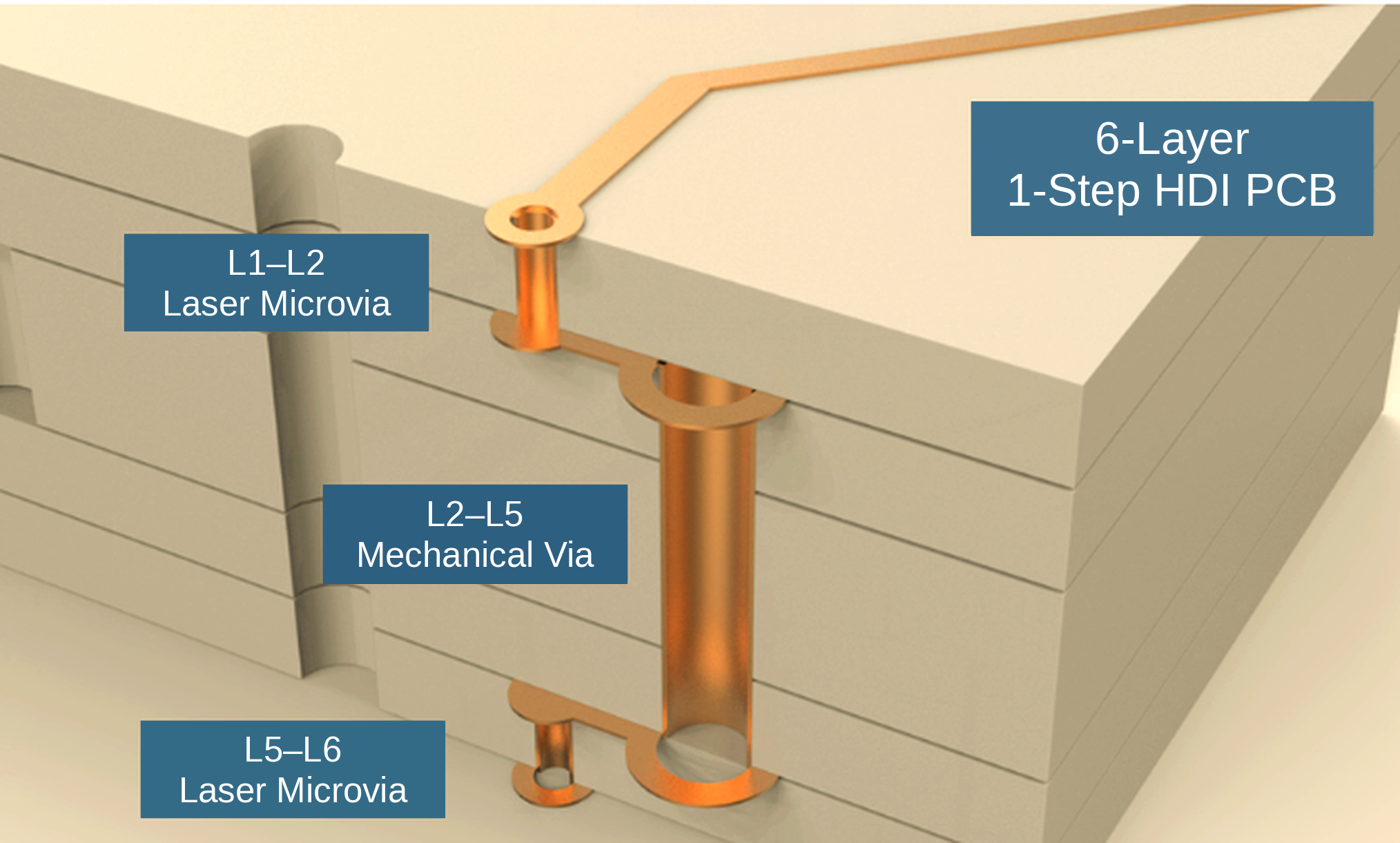
Staggered Microvias: Offset Between Levels
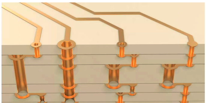
In a two-stage staggered structure, microvias in adjacent dielectric layers are offset rather than placed directly above one another. A short conductor or land connects the two levels. This can avoid putting the upper via directly on the lower via, but it uses lateral area and requires enough spacing for the capture lands, registration tolerance and the fabricator’s design rules. The lower microvia treatment still depends on the specified construction; staggered does not automatically mean unfilled.
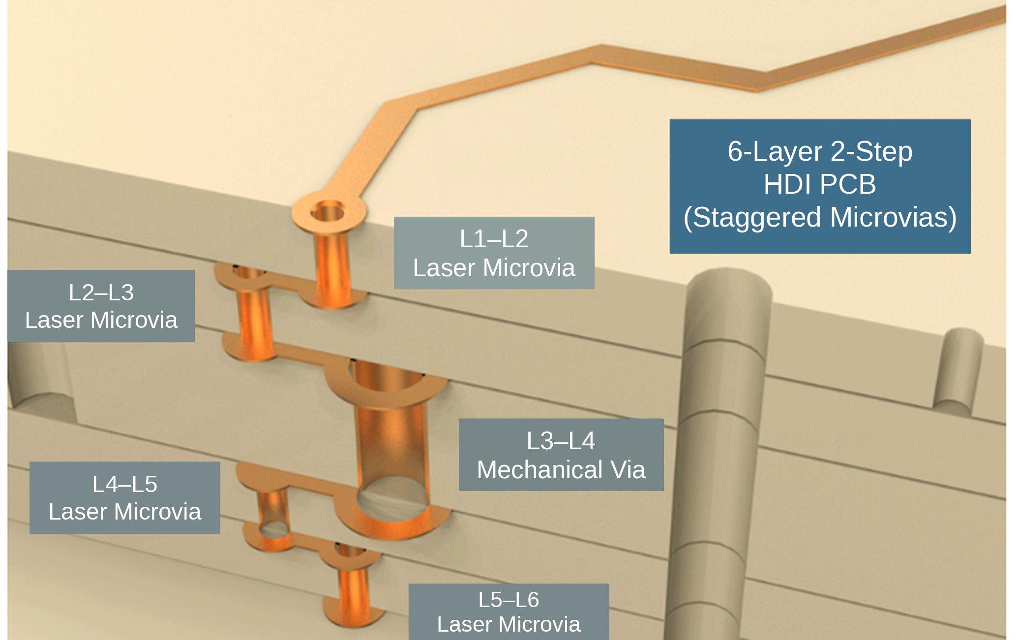
Stacked Microvias: Aligned Vertically
In a stacked structure, an upper microvia lands over a lower microvia. The arrangement can save routing area, but the lower level needs a qualified filled and planarized target so the next build-up layer can be formed reliably. Copper filling, capping, interface quality and the number of stacked levels all require review with the manufacturer. IPC has documented reliability concerns at weak microvia-to-target interfaces in complex stacked constructions; a drawing or routine visual inspection alone does not establish thermal-cycle reliability.
Files to Send for an HDI Manufacturing Review
Submit one current fabrication package with matching Gerber, NC Drill, stack-up and drawings. The PCB RFQ file checklist covers the general file and revision requirements.
- Full stack-up and via map: Identify the start and end layers for every through-hole, buried via and microvia, the required nets and component pitch, and the proposed sequential lamination and laser-drilling stages.
- Via arrangement and treatment: Mark stacked or staggered levels and specify any filling, planarization or capping, especially below another via or a solderable pad.
- Design geometry and drawings: Supply designed via diameter and depth, capture and target pad sizes, stagger spacing, registration and copper clearances, with relevant component and fabrication drawings.
- Fixed versus discussable items: Separate requirements that must be met from stack-up, via treatment or geometry that may be discussed with manufacturing engineering. Confirm the proposed process against the fabricator’s capability.
- Quotation and acceptance: State quantity and target delivery timing, plus microsection, coupon, electrical or other test and acceptance requirements appropriate to the assembly and service environment.
More advanced designs can use additional build-up stages or every-layer interconnects, but they should not be inferred from a generic multilayer drawing. The actual layer-to-layer map and process flow determine feasibility and cost.
The most useful choice is the least complex structure that meets the routing and reliability requirements. Confirm the full via map and stackup with the intended fabricator before fixing staggered or stacked microvias in the released design. For project review and quotation, request an HDI engineering review with the current file package.
BACK TO TECHNICAL ARTICLES