
Complex PCB Manufacturing · PCB Assembly · PCB Layout & DesignShenzhen, China · david.xu@mwxpcb.com

HIGH-DENSITY INTERCONNECT

HDI PCB Manufacturing

We review HDI build-up, microvia and via-in-pad construction, drill data and target impedance before quotation.

HDI Project Snapshot

Please provide Gerber or ODB++ data with drill information, the HDI stack-up and microvia definition, plus impedance notes and component constraints. We will review manufacturability before quotation.

HDI build-up

Type I–IV · 1+n+1 to 4+n+4

Interconnect options

Microvias · stacked or staggered vias · via-in-pad

Engineering review

Stack-up · drill data · impedance requirements

HDI PROJECT REVIEW

HDI Build-up & File Review

  • Build-up definition: microvia layer connections, blind or buried vias and lamination sequence are reviewed together.
  • Via and impedance review: stacked or staggered microvias, via-in-pad treatment and target impedance are checked against the design.
  • File review to quotation: submit fabrication data, drill information and HDI stack-up for manufacturability review.

Typical Applications: Telecommunications, servers, consumer electronics, data communication, industrial control, medical electronics, automotive electronics, and high-density computing.

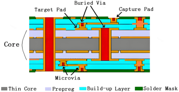
HDI PCB stack-up cross-section showing microvias, buried vias, target pads and capture pads.

MANUFACTURING DETAILS

HDI Interconnect Construction

Interconnect and Build-up Materials

Blind, buried, and plated through vias are defined by their layer connections, while microvias usually span adjacent build-up layers. The interconnect map and selected RCC or thin-core materials are reviewed together with the lamination sequence.
Stacked and Staggered Microvias

Staggered microvias are offset between levels and use lateral space for lands and routing. Stacked microvias align vertically, so the lower via typically needs filling and planarization before the next build-up layer. For more context, see stacked vs. staggered microvia review.

Via-in-Pad Construction

Via-in-pad identifies the via location within a component pad, not its treatment. For solderable pads, filling, planarization, and a copper cap can provide a flatter surface and limit solder wicking.

MANUFACTURING EXAMPLE

HDI PCB Manufacturing Example

14-layer optical-module board

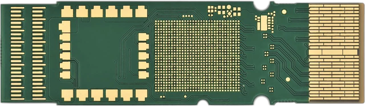
This board combines a four-step HDI build-up with via-in-pad, resin-plugged vias, controlled-depth drilling and gold fingers. Those features are coordinated in the layer build-up and drill plan.

  • 14 layers
  • Four-step HDI
  • Via-in-pad and resin-plugged vias
Fourteen-layer HDI PCB for an optical module, showing dense pads and gold fingers.

Technical Capabilities

Process ItemReference Capability
Base MaterialFR-4, Halogen Free, RCC, Ultra Thin Core, RF
Surface TreatmentENIG + OSP, ENIG, Carbon + OSP, Immersion Tin, OSP
Min. Line / Spacing2.0 / 2.0 mil
Critical Line Width Tolerance2.5 mil ±15%
Min. Microvia Drill Size (Laser)4.0 mil
Min. Capture / Target Pad Size10.0 mil
Min. PTH & Buried Drill Bit0.20 mm
Min. Annular Ring3.5 mil
Max. PTH Aspect Ratio10:1
Max. Microvia Aspect Ratio0.8:1
Single-Ended Impedance50–90 Ω: ±8% (but no less than 4 Ω)
Differential Impedance100–155 Ω: ±10%
Solder Mask Clearance1.5 mil
Solder Mask Dam2.5 mil
Min. BGA / CSP Pitch0.4 mm
Layer-to-Layer Registration2.0 mil
Min. Dielectric Thickness1.8 mil
PTH Hole Tolerance±2 mil
Min. Outline Tolerance±0.1 mm
Min. Core Thickness3.0 mil
Hole StructureStaggered Vias, Stacked Vias, Skip Vias, Stepped Vias, ELIC
HDI Type I–IV (IPC-2226A)1+n+1 … 4+n+4
Other TechnologyCarbon Jumper, LDI, DLD, Copper Filled Via, VOP

PCB Lead Time

Swipe to view all columns

PCB SpecificationOrder AreaStandard Lead TimeFastest Lead Time
4–40 Layers≤15 m²5–29 days2–17 days
4–40 Layers>15 m²Contact usContact us
Above 40 LayersAnyProject-specificProject-specific

Lead times are based on a six-day working week and exclude public holidays.

Special processes, such as heavy copper foil, peelable solder mask, and blind/buried vias, may require additional production time.

PCB lead time starts from the final confirmation of EQ.

We support 24-hour and 48-hour expedited production.

Please contact us to confirm feasibility and lead time.

All Supported Materials

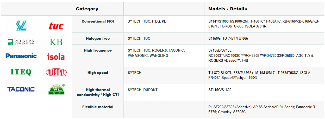
Material supplier logos including SYTECH, TUC, Rogers, KB, Panasonic, Isola, ITEQ, DuPont, Taconic and Wangling.

Swipe to view all columns

CategoryManufacturersModels / Details
Conventional FR4SYTECH, TUC, ITEQ, KBS1141/S1000H/S1000-2M; IT-158TC/IT-180ATC; KB-6160/KB-6165G/KB-6167F; TU-768/TU-865; ISOLA 370HR
Halogen freeSYTECH, TUCS1150G; TU-747T/TU-865
High frequencySYTECH, TUC, ROGERS, TACONIC, PANASONIC, WANGLINGS7135D/S7136; RO3003™/RO4003C™/RO4350B™/RO4730G3/RO5880; AGC TLY-5; ROGERS AD255C™; F4B
High speedSYTECHTU-872 SLK/TU-883/TU-933+; M-4/M-6/M-7; IT-968/IT988G; ISOLA FR408I/I-Speed®/Tachyon-100G
High thermal conductivity / High CTISYTECH, DUPONTST115G/S1600
Flexible materialPI: SF202/SF305 (Adhesive); AP-85 Series/AP-91 Series; Panasonic R-F775; Coverlay: SF305C

Send Us Your PCB Requirements

Upload your Gerber files or share your specifications for engineering review and quotation.

Email us WhatsApp Get a Quote