
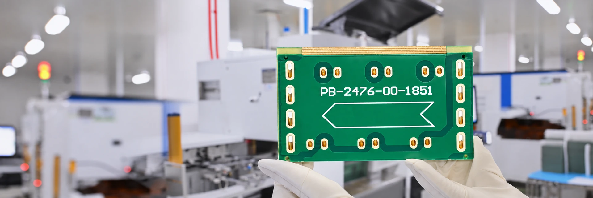
Base and Finished Copper
Base copper describes the foil entering fabrication, while finished conductor thickness reflects later plating and processing. Layer specifications distinguish nominal targets from minimum acceptance values.
HEAVY COPPER PCB
We review copper requirements by layer, current and thermal constraints, etching and plating geometry before quotation.
Please provide Gerber data and board construction, copper requirements by layer, current-path and thermal notes, critical clearances and features, and target quantity. We will review manufacturability before quotation.
Base and finished copper targets
Current paths · thermal · clearances
Gerber · construction · etch and plating feasibility
HEAVY COPPER PROJECT REVIEW
Typical Applications: Power electronics, industrial power supplies, charging systems, automotive electronics, energy equipment, and high-current control systems.
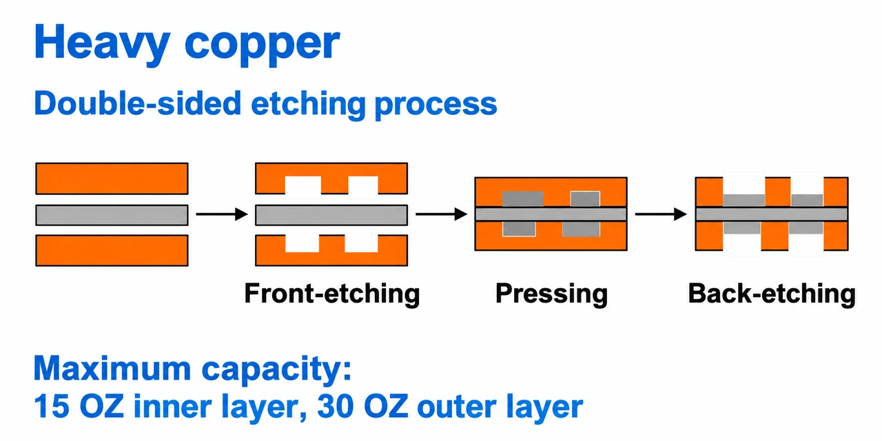
MANUFACTURING DETAILS
Base copper describes the foil entering fabrication, while finished conductor thickness reflects later plating and processing. Layer specifications distinguish nominal targets from minimum acceptance values.
Greater copper thickness changes the etching profile, so trace geometry and compensation are reviewed against the finished requirement. Plated-hole wall copper is a separate requirement from the surface conductor thickness.
Current paths are assessed with conductor width, thickness, copper distribution, connection geometry, and thermal constraints. A copper weight alone does not define the required performance without the surrounding circuit and mechanical conditions.
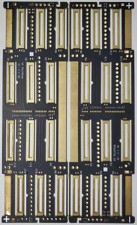
MANUFACTURING EXAMPLE
For this four-layer board, the stated copper weights correspond to approximately 105 µm inner and 175 µm outer nominal foil thickness. Etching, clearances and plating are reviewed against the required finished conductor thickness.
Swipe to view all columns
| Base copper weight | 6 oz | 8 oz | 10 oz | 12 oz |
|---|---|---|---|---|
| Minimum line width/Line space in original design(general) | 13/11 | 18/16 | 23/21 | 28/26 |
| Minimum line width/Line space of original design (limit) | (8/11.5) | (10/16) | (12/21) | (16/26) |
| Minimum line distance after compensation (limit value) | 9(8) | 11(10) | 13(12) | 15(14) |
| Compensation value (limit) | 4(3.5) | 7(6) | 10(9) | 13(12) |
| Hole to copper/hole ring to large copper ground | 12 | 14 | 16 | 18 |
Line width, spacing, clearance and compensation values are in mil. Paired values are listed as line width / spacing. Copper thickness is measured in μm; base copper weight is shown in oz in the column headings. Parenthetical values require project-specific engineering confirmation before use.
Swipe to view all columns
| PCB Specification | Order Area | Standard Lead Time | Fastest Lead Time |
|---|---|---|---|
| 4–40 Layers | ≤15 m² | 5–29 days | 2–17 days |
| 4–40 Layers | >15 m² | Contact us | Contact us |
| Above 40 Layers | Any | Project-specific | Project-specific |
Lead times are based on a six-day working week and exclude public holidays.
Special processes, such as heavy copper foil, peelable solder mask, and blind/buried vias, may require additional production time.
PCB lead time starts from the final confirmation of EQ.
We support 24-hour and 48-hour expedited production.
Please contact us to confirm feasibility and lead time.
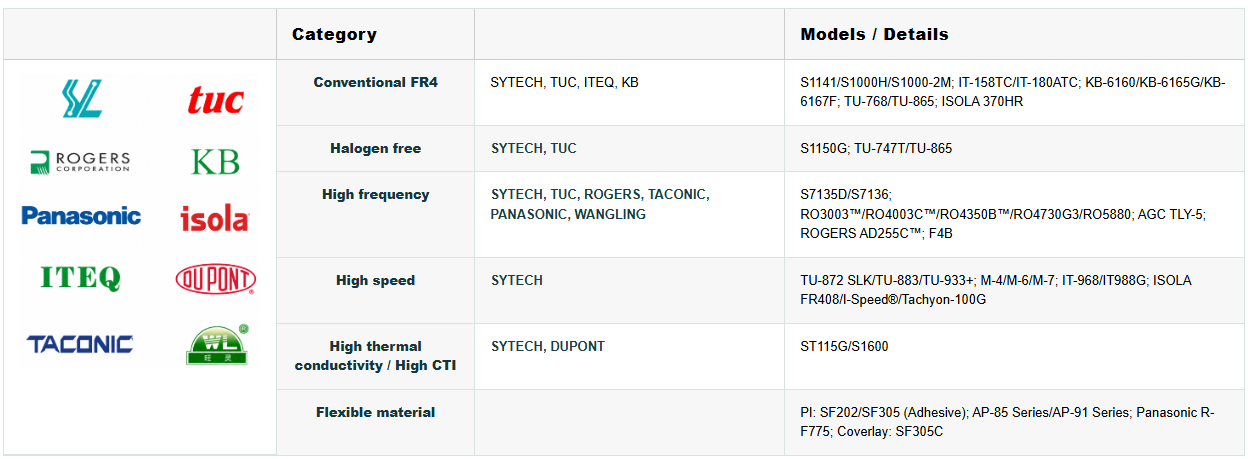
Swipe to view all columns
| Category | Manufacturers | Models / Details |
|---|---|---|
| Conventional FR4 | SYTECH, TUC, ITEQ, KB | S1141/S1000H/S1000-2M; IT-158TC/IT-180ATC; KB-6160/KB-6165G/KB-6167F; TU-768/TU-865; ISOLA 370HR |
| Halogen free | SYTECH, TUC | S1150G; TU-747T/TU-865 |
| High frequency | SYTECH, TUC, ROGERS, TACONIC, PANASONIC, WANGLING | S7135D/S7136; RO3003™/RO4003C™/RO4350B™/RO4730G3/RO5880; AGC TLY-5; ROGERS AD255C™; F4B |
| High speed | SYTECH | TU-872 SLK/TU-883/TU-933+; M-4/M-6/M-7; IT-968/IT988G; ISOLA FR408I/I-Speed®/Tachyon-100G |
| High thermal conductivity / High CTI | SYTECH, DUPONT | ST115G/S1600 |
| Flexible material | PI: SF202/SF305 (Adhesive); AP-85 Series/AP-91 Series; Panasonic R-F775; Coverlay: SF305C |
Upload your Gerber files or share your specifications for engineering review and quotation.
You can start with a simple message. No Gerber files are required.
Your message is handled according to our Privacy Policy.
If your email app did not open, copy the address below.
david.xu@mwxpcb.com