
HDI PCB Manufacturing RFQ: Build-Up, BGA, Via-in-Pad and Acceptance
An HDI quote depends on the via map, BGA escape, via-in-pad finish, impedance stackup and inspection scope.
“Eight-layer HDI board” is a starting description, not a manufacturable specification. Two boards with eight layers may need different microvia spans, lamination cycles, BGA escape routes and pad finishes. Here are five RFQ checks. For the available project scope, see HDI PCB manufacturing.
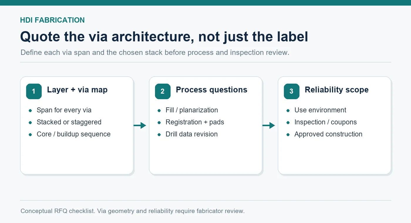
1. Map every interconnection to its start and end layers
Show the proposed stack-up and identify each plated through-hole, buried via and laser microvia by its actual layer span—for example, L1–L2 rather than “blind via” alone. Indicate whether multiple build-up stages are needed and where the layers are added. Flag conflicts among artwork, drill table and fabrication drawing as provisional.
For each laser microvia, provide the proposed diameter, dielectric depth, capture and target pads, and required surface treatment. Review its depth-to-diameter relationship separately from the aspect ratio of mechanically drilled plated holes. A mechanical-hole capability limit does not establish a laser-microvia capability, or vice versa. The manufacturing partner assigned to the project must confirm the construction against its actual process and materials.
2. Check BGA escape and controlled impedance together
A fine-pitch BGA may force a via into a component pad or require routing on an additional build-up layer. Supply the component land pattern and pitch, the proposed fanout, any no-via areas, and the nets that require controlled impedance. A pad that appears routable in CAD may still leave insufficient room for capture lands, copper clearance or registration tolerance.
The impedance table should identify target values, tolerances, reference planes and the affected traces. Also distinguish starting copper from required finished conductor thickness. Changing dielectric thickness to make a microvia buildable can change the trace geometry needed for impedance; the via plan and stack-up should therefore be reviewed as one design. A generic “50 Ω” note cannot settle all these choices.
3. State what happens to vias in solderable pads
“Via-in-pad” identifies location, not the finished pad surface. Mark which BGA or other solderable pads contain vias and specify whether each construction needs filling, planarization and a plated cap. An open pad via can complicate soldering; filling and planarization add process and inspection requirements. The appropriate treatment depends on whether the feature is a laser microvia or another via type, the pad geometry and the assembly process.
If one microvia lands on another, identify that relationship in the via map rather than relying on the word “stacked.” The existing stacked versus staggered microvia guide explains those layouts in detail. Here, the RFQ decision is to name the proposed fill and surface requirements, then ask manufacturing engineering to confirm a qualified build route.
4. Separate prototype assumptions from volume requirements
State the prototype quantity and the expected follow-on volume, but do not assume a prototype quote automatically qualifies the same design for repeat production. Ask which material, build-up sequence, microvia treatment, surface finish and test method will remain the same. If a prototype uses a temporary material or simplified acceptance plan, identify that difference before treating its price or lead time as a volume baseline.
Record any design changes after the prototype: BGA package, stack-up, via spans, impedance table and assembly profile can each alter the manufacturing review. MWX PCB can coordinate the file and question exchange; the manufacturing partner's engineering team confirms process feasibility and production-specific conditions.
5. Agree on the RFQ package and acceptance evidence
Send one revision-controlled package containing fabrication data, drill information, the stack-up and via map, component constraints, impedance requirements, quantity and requested timing. State the surface finish and any customer-specific standard or operating environment. If microsections, electrical tests, impedance coupons or additional thermal-stress evidence are required, specify the method and acceptance criteria for quotation. IPC has documented latent failures at weak microvia interfaces that routine bare-board inspection alone may miss; the appropriate test plan needs agreement for the actual application.
You can begin an HDI PCB RFQ even when final Gerbers are not ready: the website form does not require file upload. Describe the current build-up idea, BGA constraint, quantities and open decisions in the project details, and label each item that still needs engineering confirmation. A formal production quote should follow the agreed construction and current files, not an inferred capability from the layer count.
BACK TO TECHNICAL ARTICLES