
RF PCB Insertion Loss: Why Df Alone Cannot Predict the Finished Board
Compare dielectric, conductor and test-path effects before specifying an RF PCB insertion-loss target.
A low dissipation factor (Df) is useful when selecting an RF laminate, but it is not an insertion-loss specification for a finished PCB. A 50-ohm transmission line also has a width, copper surface, dielectric thickness, surface finish where applied, length and operating frequency. Changing any of these can change the measured result even when the laminate name stays the same. This article explains what to compare before requesting an RF manufacturing review.
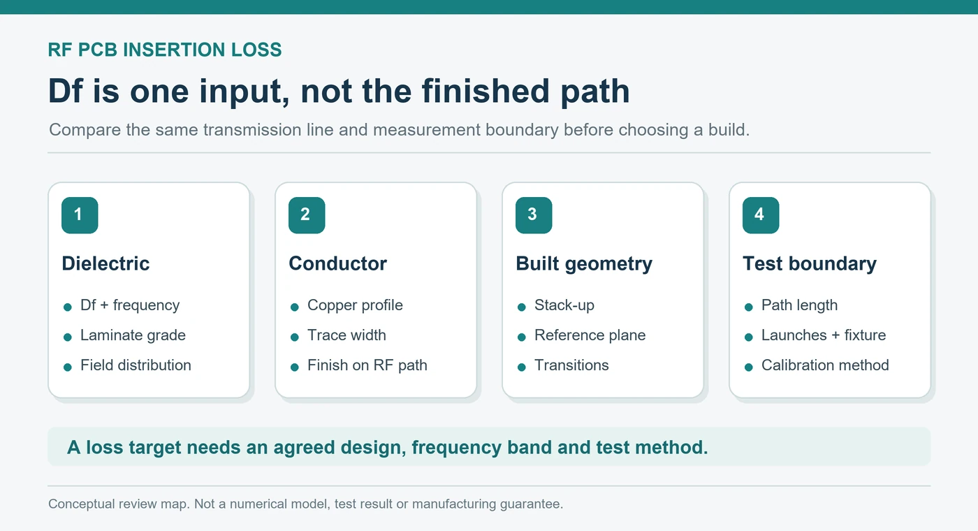
Start with the path being measured
Insertion loss describes the reduction in transmitted signal through a defined path. On a test board, the reported S21 may include the line, transitions, launches, connectors and fixture unless the measurement method removes or separates them. A board trace measured over one length or frequency band cannot be fairly compared with a different trace or test setup by looking at the final dB number alone.
For a simple transmission line, dielectric and conductor loss are often the main material-and-construction contributions. Radiation, leakage, discontinuities and mismatch can also matter for a particular layout or measurement. The purpose of separating these effects is to find the design or fabrication variable that can actually be changed, not to claim that every effect can be calculated from a laminate datasheet.
Df describes a material contribution, with test conditions
Df helps estimate dielectric loss, but its quoted value belongs to a stated frequency and test method. The electric field also depends on line type and stack-up: a microstrip and a stripline do not interact with the dielectric in the same way. A material comparison should therefore use the intended frequency range, laminate grade, thickness and transmission-line construction. Our Rogers material selection guide explains why a single Dk or Df number is insufficient to choose an RF build.
Lower Df may reduce one part of the loss budget. It does not automatically outweigh a change in conductor width, copper profile or finish. The complete proposed construction should be modeled and reviewed before a material substitution is approved.
Conductor loss depends on the built copper geometry
At high frequency, current distribution and copper surface condition affect conductor loss. A rougher copper-to-dielectric interface can increase it. Width matters too: for the same line type and other fixed inputs, a thinner dielectric may require a narrower trace to keep the same target impedance, increasing the conductor contribution even though the laminate Df is unchanged. Foil type, finished copper thickness and any finish on exposed RF traces should be specified where they are critical to the design.
Fabrication can alter the intended cross-section through etching, plating and lamination. The released impedance geometry and the as-built line therefore need to be discussed together. This does not mean one copper or finish choice is best for every RF layout; its effect depends on the line structure, frequency and acceptance target.
Compare alternatives against the same reference design
If two constructions are being evaluated, keep the comparison conditions visible:
- Electrical target: frequency band, reference impedance, maximum acceptable loss and the relevant net or coupon structure.
- Physical path: microstrip, stripline or another line type; trace length, layer and reference plane; width and spacing.
- Materials and build: laminate grade, dielectric thickness, copper type or profile, finished copper and surface finish where it touches the RF path.
- Test boundary: whether launches, connectors and fixtures remain in the measurement, and whether the result is reported for the whole path or per unit length.
For example, a material with a lower published Df may still produce more measured loss in a different, narrower line construction. That is a comparison problem, not evidence that the datasheet is wrong. Ask for the same geometry and measurement basis, or identify why the designs cannot be directly compared.
Agree on verification before quoting a loss target
State the proposed frequency range, test structure, calibration or fixture-removal method, reporting units and acceptance limit. Decide whether a test coupon represents the actual critical RF line and which transitions are included. A vector network analyzer result for the entire assembled path is useful, but it should not be described as the PCB laminate loss alone.
For manufacturing review, provide the stack-up, controlled-impedance table, critical RF geometry, material and copper requirements, surface-finish areas, quantities and any required insertion-loss test. The RF manufacturing RFQ guide explains how to keep these inputs in one quotation baseline. The assigned manufacturing partner must confirm what construction and verification method are feasible for the actual project.
See RF and microwave PCB manufacturing for the product scope. You can send an RF PCB enquiry with the operating band, proposed material, layer build, critical line and open loss questions even if the final fabrication package is still being prepared. Mark provisional items clearly; no universal insertion-loss figure should be inferred from a material grade alone.
BACK TO TECHNICAL ARTICLES